AD9271BSVZRL-25 Analog Devices Inc, AD9271BSVZRL-25 Datasheet - Page 34
AD9271BSVZRL-25
Manufacturer Part Number
AD9271BSVZRL-25
Description
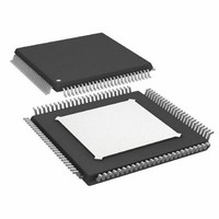
IC ADC OCT 12BIT 25MSPS 100-TQFP
Manufacturer
Analog Devices Inc
Datasheet
1.AD9271BSVZ-50.pdf
(60 pages)
Specifications of AD9271BSVZRL-25
Number Of Bits
12
Sampling Rate (per Second)
25M
Data Interface
Serial, SPI™
Number Of Converters
8
Power Dissipation (max)
1.06W
Voltage Supply Source
Single Supply
Operating Temperature
-40°C ~ 85°C
Mounting Type
Surface Mount
Package / Case
100-TQFP Exposed Pad
Power Dissipation Pd
150mW
Peak Reflow Compatible (260 C)
Yes
Supply Voltage
1.8V
Sample Rate
25 MSPS
Termination Type
SMD
Supply Voltage Max
1.9V
Input Channels Per Adc
8
Lead Free Status / RoHS Status
Lead free / RoHS Compliant
For Use With
AD9271-50EBZ - BOARD EVALUATION AD9271 50MSPS
Lead Free Status / RoHS Status
Lead free / RoHS Compliant, Lead free / RoHS Compliant
Available stocks
Company
Part Number
Manufacturer
Quantity
Price
Company:

Part Number:
AD9271BSVZRL-25
Manufacturer:
AD
Quantity:
1 140
Company:
Part Number:
AD9271BSVZRL-25
Manufacturer:
Analog Devices Inc
Quantity:
10 000


AD9271
Internal Reference Operation
A comparator within the AD9271 detects the potential at the
SENSE pin and configures the reference. If SENSE is grounded,
the reference amplifier switch is connected to the internal
resistor divider (see Figure 66), setting VREF to 1 V.
The REFT and REFB pins establish their input span of the ADC
core from the reference configuration. The analog input full-
scale range of the ADC equals twice the voltage at the reference
pin for either an internal or an external reference configuration.
1µF
*OPTIONAL.
1µF*
REFERENCE
EXTERNAL
SENSE
0.1µF
SENSE
0.1µF*
VREF
VIN+
VIN–
VREF
AVDD
VIN+
VIN–
Figure 66. Internal Reference Configuration
Figure 67. External Reference Operation
SELECT
LOGIC
SELECT
LOGIC
CORE
ADC
CORE
ADC
0.5V
0.5V
REFT
REFB
REFT
REFB
0.1µF
0.1µF
0.1µF
0.1µF
0.1µF
0.1µF
+
+
4.7µF
4.7µF
Rev. B | Page 34 of 60
External Reference Operation
The use of an external reference may be necessary to enhance
the gain accuracy of the ADC or to improve thermal drift charac-
teristics. Figure 69 shows the typical drift characteristics of the
internal reference in 1 V mode.
When the SENSE pin is tied to AVDD, the internal reference is
disabled, allowing the use of an external reference. The external
reference is loaded with an equivalent 6 kΩ load. An internal
reference buffer generates the positive and negative full-scale
references, REFT and REFB, for the ADC core. Therefore, the
external reference must be limited to a nominal voltage of 1.0 V.
–0.02
–0.04
–0.06
–0.08
–0.10
–0.12
–0.14
–0.16
–0.18
–0.20
0.02
–10
–15
–20
–25
–5
5
0
0
–40
0
Figure 68. VREF Accuracy vs. Load, AD9271-50
Figure 69. Typical VREF Drift, AD9271-50
0.5
–20
1.0
0
CURRENT LOAD (mA)
TEMPERATURE (°C)
1.5
20
2.0
40
2.5
60
3.0
80
3
.5
Related parts for AD9271BSVZRL-25
Image
Part Number
Description
Manufacturer
Datasheet
Request
R

Part Number:
Description:
Octal LNA/VGA/AAF/ADC and Crosspoint Switch
Manufacturer:
Analog Devices
Datasheet:

Part Number:
Description:
BOARD EVALUATION AD9271 50MSPS
Manufacturer:
Analog Devices Inc
Datasheet:

Part Number:
Description:
±1.7g Dual-Axis IMEMS Accelerometer Evaluation Board
Manufacturer:
Analog Devices Inc
Datasheet:
Part Number:
Description:
Inertial Sensor Evaluation System
Manufacturer:
Analog Devices Inc
Datasheet:
Part Number:
Description:
Manufacturer:
Analog Devices Inc
Datasheet:
Part Number:
Description:
Manufacturer:
Analog Devices Inc
Datasheet:
Part Number:
Description:
Manufacturer:
Analog Devices Inc
Datasheet:
Part Number:
Description:
Manufacturer:
Analog Devices Inc
Datasheet:
Part Number:
Description:
Manufacturer:
Analog Devices Inc
Datasheet:
Part Number:
Description:
Manufacturer:
Analog Devices Inc
Datasheet:
Part Number:
Description:
Manufacturer:
Analog Devices Inc
Datasheet:
Part Number:
Description:
Manufacturer:
Analog Devices Inc
Datasheet:
Part Number:
Description:
Manufacturer:
Analog Devices Inc
Datasheet: