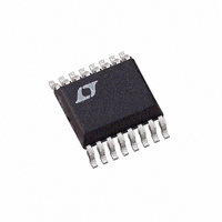
LTC1417ACGN Linear Technology, LTC1417ACGN Datasheet - Page 7

LTC1417ACGN
Manufacturer Part Number
LTC1417ACGN
Description
IC A/D CONV 14BIT SAMPLNG 16SSOP
Manufacturer
Linear Technology
Datasheet
1.LTC1417CGNPBF.pdf
(32 pages)
Specifications of LTC1417ACGN
Number Of Bits
14
Sampling Rate (per Second)
400k
Data Interface
MICROWIRE™, Serial, SPI™
Number Of Converters
1
Power Dissipation (max)
27.5mW Unipolar; 44mW Bipolar
Voltage Supply Source
Dual ±
Operating Temperature
0°C ~ 70°C
Mounting Type
Surface Mount
Package / Case
16-SSOP (0.150", 3.90mm Width)
Lead Free Status / RoHS Status
Contains lead / RoHS non-compliant
Available stocks
Company
Part Number
Manufacturer
Quantity
Price
Company:
Part Number:
LTC1417ACGN
Manufacturer:
LT
Quantity:
10 000
Part Number:
LTC1417ACGN
Manufacturer:
LTNEAR
Quantity:
20 000
Company:
Part Number:
LTC1417ACGN#PBF
Manufacturer:
CYPRESS
Quantity:
120
Part Number:
LTC1417ACGN#PBF
Manufacturer:
LINEAR/凌特
Quantity:
20 000
Company:
Part Number:
LTC1417ACGN#TRPBF
Manufacturer:
LT
Quantity:
450
PIN
TYPICAL PERFOR A CE CHARACTERISTICS
A
A
V
with 1 F.
REFCOMP (Pin 4): 4.096V Reference Output. Bypass to
AGND using 10 F tantalum in parallel with 0.1 F ceramic.
AGND (Pin 5): Analog Ground.
EXTCLKIN (Pin 6): External Conversion Clock Input. A 5V
input will enable the internal conversion clock.
SCLK (Pin 7): Data Clock Input.
IN
IN
REF
5.0
4.5
4.0
3.5
3.0
2.5
2.0
1.5
1.0
0.5
U
+
–
6
5
4
3
2
1
0
0
–75
(Pin 1): Positive Analog Input.
(Pin 2): Negative Analog Input.
(Pin 3): 2.50V Reference Output. Bypass to AGND
V
Temperature (Unipolar Mode)
V
Frequency (Unipolar Mode)
0
DD
DD
FUNCTIONS
–50
50
Supply Current vs
Supply Current vs Sampling
100
U
–25
SAMPLING FREQUENCY (kHz)
150
TEMPERATURE ( C)
0
200
25
250
U
50
300 350
75
100 125
W
400 450
1417 G13
1417 G16
U
150
500
5.0
4.5
4.0
3.5
3.0
2.5
2.0
1.5
1.0
0.5
6
5
4
3
2
1
0
0
–75
0
V
Frequency (Bipolar Mode)
V
Temperature (Bipolar Mode)
DD
DD
–50
50
Supply Current vs
Supply Current vs Sampling
100
–25
SAMPLING FREQUENCY (kHz)
150
TEMPERATURE ( C)
0
200
25
250
CLKOUT (Pin 8): Conversion Clock Output.
D
DGND (Pin 10): Digital Ground.
SHDN (Pin 11): Power Shutdown Input. Low selects
shutdown. Shutdown mode selected by RD. RD = 0V for
Nap mode and RD = 5V for Sleep mode.
RD (Pin 12): Read Input. This enables the output drivers.
RD also sets the shutdown mode when SHDN goes low.
RD and SHDN low selects the quick wake-up Nap mode,
RD high and SHDN low selects Sleep mode.
50
OUT
300 350
75
(Pin 9): Serial Data Output.
100 125
400 450
(T
1417 G14
1417 G17
A
= 25 C, unless otherwise specified)
150
500
3.0
2.5
2.0
1.5
1.0
0.5
2.5
2.0
1.5
1.0
0.5
0
0
–75
0
V
Temperature (Bipolar Mode)
V
Frequency (Bipolar Mode)
SS
SS
–50
50
Supply Current vs
Supply Current vs Sampling
100
–25
SAMPLING FREQUENCY (kHz)
150
TEMPERATURE ( C)
0
200
25
250
LTC1417
50
300 350
75
sn1417 1417fas
100 125
400 450
1417 G15
1417 G18
7
150
500


