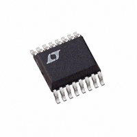
LTC1417ACGN Linear Technology, LTC1417ACGN Datasheet - Page 3

LTC1417ACGN
Manufacturer Part Number
LTC1417ACGN
Description
IC A/D CONV 14BIT SAMPLNG 16SSOP
Manufacturer
Linear Technology
Datasheet
1.LTC1417CGNPBF.pdf
(32 pages)
Specifications of LTC1417ACGN
Number Of Bits
14
Sampling Rate (per Second)
400k
Data Interface
MICROWIRE™, Serial, SPI™
Number Of Converters
1
Power Dissipation (max)
27.5mW Unipolar; 44mW Bipolar
Voltage Supply Source
Dual ±
Operating Temperature
0°C ~ 70°C
Mounting Type
Surface Mount
Package / Case
16-SSOP (0.150", 3.90mm Width)
Lead Free Status / RoHS Status
Contains lead / RoHS non-compliant
Available stocks
Company
Part Number
Manufacturer
Quantity
Price
Company:
Part Number:
LTC1417ACGN
Manufacturer:
LT
Quantity:
10 000
Part Number:
LTC1417ACGN
Manufacturer:
LTNEAR
Quantity:
20 000
Company:
Part Number:
LTC1417ACGN#PBF
Manufacturer:
CYPRESS
Quantity:
120
Part Number:
LTC1417ACGN#PBF
Manufacturer:
LINEAR/凌特
Quantity:
20 000
Company:
Part Number:
LTC1417ACGN#TRPBF
Manufacturer:
LT
Quantity:
450
DY A IC ACCURACY
I TER AL REFERE CE CHARACTERISTICS
DIGITAL I PUTS A D DIGITAL OUTPUTS
A ALOG I PUT
otherwise specifications are at T
SYMBOL PARAMETER
C
t
t
t
CMRR
operating temperature range, otherwise specifications are at T
PARAMETER
V
V
V
V
operating temperature range, otherwise specifications are at T
otherwise specifications are at T
SYMBOL
S/(N + D)
THD
SFDR
IMD
SYMBOL PARAMETER
V
V
I
C
V
V
I
C
I
I
ACQ
AP
jitter
IN
OZ
SOURCE
SINK
U
IN
REF
REF
REF
REF
IH
IL
IN
OH
OL
OZ
U
Output Voltage
Output Tempco
Line Regulation
Output Resistance
U W
Analog Input Capacitance
Sample-and-Hold Acquisition Time
Sample-and-Hold Aperture Time
Sample-and-Hold Aperture Time Jitter
Analog Input Common Mode Rejection Ratio
High Level Input Voltage
Low Level Input Voltage
Digital Input Current
Digital Input Capacitance
High Level Output Voltage
Low Level Output Voltage
High-Z Output Leakage D
High-Z Output Capacitance D
Output Source Current
Output Sink Current
U
PARAMETER
Signal-to-(Noise + Distortion) Ratio
Total Harmonic Distortion
Spurious Free Dynamic Range
Intermodulation Distortion
Full Power Bandwidth
Full Linear Bandwidth
U
U
CONDITIONS
I
I
I
4.75V V
– 5.25V V
0.1mA
OUT
OUT
OUT
The
OUT
A
A
U
U
= 25 C. (Note 5)
= 25 C. (Note 5)
= 0
= 0, 0 C T
= 0, – 40 C T
, CLKOUT
OUT
indicates specifications which apply over the full operating temperature range,
|
, CLKOUT
DD
I
OUT
SS
The
|
5.25V
– 4.75V
A
0.1mA
indicates specifications which apply over the full operating temperature range,
A
CONDITIONS
100kHz Input Signal
100kHz Input Signal, First Five Harmonics
200kHz Input Signal
f
S/(N + D) 77dB
70 C
IN1
85 C
= 97.3kHz, f
CONDITIONS
Between Conversions (Sample Mode)
During Conversions (Hold Mode)
0V < (A
– 2.048V < (A
CONDITIONS
V
V
V
V
V
V
V
V
RD High (Note 9)
V
V
DD
DD
IN
DD
DD
DD
DD
OUT
OUT
OUT
= 0V to V
= 5.25V
= 4.75V
= 4.75V, I
= 4.75V, I
= 4.75V, I
= 4.75V, I
= 0V to V
= 0V
= V
IN
DD
+
IN2
= A
A
A
DD
= 25 C. (Note 5)
IN
= 25 C. (Note 5)
IN
= 104.6kHz
O
O
O
O
DD
+
–
= – 10 A
= – 200 A
= 160 A
= – 1.6mA
= A
) < 4.096V (Unipolar)
, RD High
IN
–
) < 2.048V (Bipolar)
The
The
indicates specifications which apply over the full
indicates specifications which apply over the full
2.480
MIN
MIN
MIN
– 85
2.4
4.0
79
MIN
2.500
0.05
0.05
4.74
0.05
0.10
TYP
– 95
– 98
– 97
TYP
TYP
– 10
0.8
1.4
10
10
81
8
10
20
–1.5
TYP
150
14
65
65
3
5
LTC1417
2.520
MAX
MAX
MAX
0.8
0.4
15
MAX
10
10
500
sn1417 1417fas
ppm/ C
ppm/ C
UNITS
UNITS
UNITS
LSB/V
LSB/V
UNITS
ps
3
MHz
MHz
RMS
mA
mA
k
dB
dB
dB
dB
dB
dB
pF
pF
ns
ns
pF
pF
V
V
V
A
V
V
V
V
A


