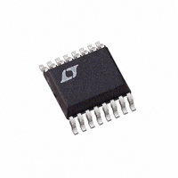
LTC1417ACGN Linear Technology, LTC1417ACGN Datasheet - Page 25

LTC1417ACGN
Manufacturer Part Number
LTC1417ACGN
Description
IC A/D CONV 14BIT SAMPLNG 16SSOP
Manufacturer
Linear Technology
Datasheet
1.LTC1417CGNPBF.pdf
(32 pages)
Specifications of LTC1417ACGN
Number Of Bits
14
Sampling Rate (per Second)
400k
Data Interface
MICROWIRE™, Serial, SPI™
Number Of Converters
1
Power Dissipation (max)
27.5mW Unipolar; 44mW Bipolar
Voltage Supply Source
Dual ±
Operating Temperature
0°C ~ 70°C
Mounting Type
Surface Mount
Package / Case
16-SSOP (0.150", 3.90mm Width)
Lead Free Status / RoHS Status
Contains lead / RoHS non-compliant
Available stocks
Company
Part Number
Manufacturer
Quantity
Price
Company:
Part Number:
LTC1417ACGN
Manufacturer:
LT
Quantity:
10 000
Part Number:
LTC1417ACGN
Manufacturer:
LTNEAR
Quantity:
20 000
Company:
Part Number:
LTC1417ACGN#PBF
Manufacturer:
CYPRESS
Quantity:
120
Part Number:
LTC1417ACGN#PBF
Manufacturer:
LINEAR/凌特
Quantity:
20 000
Company:
Part Number:
LTC1417ACGN#TRPBF
Manufacturer:
LT
Quantity:
450
*
*
*
GETDATAPSHX
*
*****************************************
* Setup indecies
*****************************************
*
*
*
*****************************************
* The next short loop ensures that the
* LTC1417’s conversion is finished
* before starting the SPI data transfer *
*****************************************
*
CONVENDLDAA
*
*
*
*
*
*************************************************************************
* This routine sends data to the LTC1417 and sets its MUX channel. The
* very first time this routine is entered produces invalid data. Each
* time thereafter, the data will correspond to the previous active
* CONVST signal sent to the LTC1417.
*************************************************************************
*
*
*
WAITMX1 LDAA
*
*
WAITMX2 LDAA
*
*
*
*
TYPICAL APPLICATIONS
PSHY
PSHA
LDX
LDY
ANDA
BPL
LDAA
BCLR
STAA
BPL
LDAA
STAA
LDAA
ORAA
STAA
BPL
BSET
LDAA
STAA
LDD
LSRD
LSRD
STD
#$0
#$1000
PORTC
#%10000000
CONVEND
#$00
PORTD,Y %00100000
SPDR
SPSR
WAITMX1If the transfer is not finished, read status
SPDR
DIN1
MUX
#$08
SPDR
SPSR
WAITMX2If the transfer is not finished, read status
PORTD,Y %00100000
SPDR
DIN2
DIN1
DIN1
(This assumes an E-Clock frequency of 4MHz. For higher
E-Clock frequencies, change the above value of $50 to a
value that ensures the SCK frequency is 2MHz or less.)
The X register is used as a pointer to the memory
locations that hold the conversion data
Dummy value for upper byte of 16-bit SPI transfer
Transfer Accum. A contents to SPI register to initiate
serial transfer
Get SPI transfer status
Load accumulator A with the current byte of LTC1417 data
that was just received
Transfer the LTC1417’s high byte (Bit13 - Bit6) to memory
Retrieve MUX address
Set the MUX’s ENABLE bit
Transfer Accum. A contents to SPI register to initiate
serial transfer
Get SPI transfer status
Load accumulator A with the current byte of LTC1417 data
that was just received
Transfer the LTC1417’s low byte (Bit5 - Bit0) to memory
Load the contents of DIN1 and DIN2 into the double
accumulator D
Two logical shifts to the right to right justify the
14-bit conversion results
Place right justified result back in memory
Retrieve the contents of port D
Look at Bit7
Bit7 = Hi; the LTC1417’s conversion is complete
Bit7 = Lo; the LTC1417’s conversion is not
complete
Branch to the loop’s beginning while Bit7 remains
low
U
This sets the SS* output bit to a logic
low, selecting the LTC1417
This sets the SS* output bit to a logic
high, de-selecting the LTC1417
*
*
*
*
*
*
*
LTC1417
sn1417 1417fas
25


