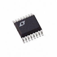
LTC1417ACGN Linear Technology, LTC1417ACGN Datasheet - Page 30

LTC1417ACGN
Manufacturer Part Number
LTC1417ACGN
Description
IC A/D CONV 14BIT SAMPLNG 16SSOP
Manufacturer
Linear Technology
Datasheet
1.LTC1417CGNPBF.pdf
(32 pages)
Specifications of LTC1417ACGN
Number Of Bits
14
Sampling Rate (per Second)
400k
Data Interface
MICROWIRE™, Serial, SPI™
Number Of Converters
1
Power Dissipation (max)
27.5mW Unipolar; 44mW Bipolar
Voltage Supply Source
Dual ±
Operating Temperature
0°C ~ 70°C
Mounting Type
Surface Mount
Package / Case
16-SSOP (0.150", 3.90mm Width)
Lead Free Status / RoHS Status
Contains lead / RoHS non-compliant
Available stocks
Company
Part Number
Manufacturer
Quantity
Price
Company:
Part Number:
LTC1417ACGN
Manufacturer:
LT
Quantity:
10 000
Part Number:
LTC1417ACGN
Manufacturer:
LTNEAR
Quantity:
20 000
Company:
Part Number:
LTC1417ACGN#PBF
Manufacturer:
CYPRESS
Quantity:
120
Part Number:
LTC1417ACGN#PBF
Manufacturer:
LINEAR/凌特
Quantity:
20 000
Company:
Part Number:
LTC1417ACGN#TRPBF
Manufacturer:
LT
Quantity:
450
LTC1417
TYPICAL APPLICATIONS
*
TRFLP1 LDAA
*
WAIT1
*
*
*
*
*
*
*
*
CONVST
30
BUSY
DATA
SCLK
D
MUX
OUT
RD
Figure 24. Using the Sample Program In Listing 2, the LTC1417, Combined with the DG408 8-Channel MUX,
Has No Latency Between the Selected Input Voltage and Its Conversion Data as Shown In the Timing Relationship Above
BCLR
STAA
LDAA
BPL
LDAA
STAA
INX
CPX
BNE
BSET
LDD
LSRD
LSRD
STD
PULA
PULY
PULX
RTS
PORTD,Y %00100000
#$0
SPDR
SPSR
WAIT1
SPDR
0,X
#DIN2+1Has the last byte been transferred/exchanged?
TRFLP1 If the last byte has not been reached, then proceed to
PORTD,Y %00100000
DIN1
DIN1
CH0
Load accumulator A with a null byte for SPI transfer
This writes the byte into the SPI data register and
starts the transfer
This loop waits for the SPI to complete a serial
transfer/exchange by reading the SPI Status Register
The SPIF (SPI transfer complete flag) bit is the SPSR’s
MSB and is set to one at the end of an SPI transfer. The
branch will occur while SPIF is a zero.
Load accumulator A with the current byte of LTC1417 data
that was just received
Transfer the LTC1417’s data to memory
Increment the pointer
the next byte for transfer/exchage
Load the contents of DIN1 and DIN2 into the double
accumulator D
Two logical shifts to right justify the 14-bit
conversion results
Return right justified data to memory
Restore the A register
Restore the Y register
Restore the X register
CH0 DATA
U
This sets the SS* output bit to a logic
low, selecting the LTC1417
This sets the SS* output bit to a logic
high, de-selecting the LTC1417
CH1
CH1 DATA
CH2
CH2 DATA
CH3
CH3 DATA
CH5
sn1417 1417fas
1417 F24


