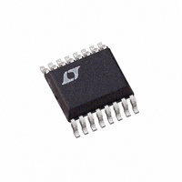
LTC1417ACGN Linear Technology, LTC1417ACGN Datasheet - Page 15

LTC1417ACGN
Manufacturer Part Number
LTC1417ACGN
Description
IC A/D CONV 14BIT SAMPLNG 16SSOP
Manufacturer
Linear Technology
Datasheet
1.LTC1417CGNPBF.pdf
(32 pages)
Specifications of LTC1417ACGN
Number Of Bits
14
Sampling Rate (per Second)
400k
Data Interface
MICROWIRE™, Serial, SPI™
Number Of Converters
1
Power Dissipation (max)
27.5mW Unipolar; 44mW Bipolar
Voltage Supply Source
Dual ±
Operating Temperature
0°C ~ 70°C
Mounting Type
Surface Mount
Package / Case
16-SSOP (0.150", 3.90mm Width)
Lead Free Status / RoHS Status
Contains lead / RoHS non-compliant
Available stocks
Company
Part Number
Manufacturer
Quantity
Price
Company:
Part Number:
LTC1417ACGN
Manufacturer:
LT
Quantity:
10 000
Part Number:
LTC1417ACGN
Manufacturer:
LTNEAR
Quantity:
20 000
Company:
Part Number:
LTC1417ACGN#PBF
Manufacturer:
CYPRESS
Quantity:
120
Part Number:
LTC1417ACGN#PBF
Manufacturer:
LINEAR/凌特
Quantity:
20 000
Company:
Part Number:
LTC1417ACGN#TRPBF
Manufacturer:
LT
Quantity:
450
APPLICATIONS
wait state during conversion or by using three-state buff-
ers to isolate the ADC data bus. The traces connecting the
pins and bypass capacitors must be kept short and should
be made as wide as possible.
The LTC1417 has differential inputs to minimize noise
coupling. Common mode noise on the A
will be rejected by the input CMRR. The A
used as a ground sense for the A
hold and convert the difference voltage between A
A
kept as short as possible. In applications where this is not
possible, the A
side to equalize coupling.
SUPPLY BYPASSING
High quality, low series resistance ceramic, 10 F bypass
capacitors should be used at the V
Surface mount ceramic capacitors such as Taiyo Yuden
LMK325BJ106MN provide excellent bypassing in a small
board space. Alternatively 10 F tantalum capacitors in
parallel with 0.1 F ceramic capacitors can be used.
Bypass capacitors must be located as close to the pins as
possible. The traces connecting the pins and the bypass
capacitors must be kept short and should be made as wide
as possible.
IN
–
. The leads to A
IN
+
and A
U
IN
CIRCUITRY
+
ANALOG
(Pin 1) and A
INPUT
IN
INFORMATION
U
–
traces should be run side by
+
–
1
IN
A
IN
+
DD
2
+
input; the LTC1417 will
A
W
IN
IN
–
and REFCOMP pins.
–
Figure 14. SHDN to CONVST Wake-Up Timing
V
IN
Figure 12. Power Supply Grounding Practice
(Pin 2) should be
REF
+
IN
3
CONVST
1 F
and A
SHDN
–
input can be
ANALOG GROUND PLANE
REFCOMP
U
IN
4
IN
–
10 F
leads
+
and
AGND
LTC1417
t
1
5
Example Layout
Figures 13a, 13b, 13c and 13d show the schematic and
layout of a suggested evaluation board. The layout demon-
strates the proper use of decoupling capacitors and ground
plane with a 2-layer printed circuit board.
POWER SHUTDOWN
The LTC1417 provides two power shutdown modes, Nap
and Sleep, to save power during inactive periods. The
Nap mode reduces ADC power dissipation by 80% and
leaves only the digital logic and reference powered up.
The wake-up time from Nap to active is 500ns (see Figure
14). In Sleep mode, all bias currents are shut down and
only leakage current remains— about 2 A. Wake-up
time from Sleep mode is much slower since the reference
circuit must power up and settle to 0.005% for full 14-bit
accuracy. Sleep mode wake-up time is dependent on the
value of the capacitor connected to the REFCOMP (Pin 4).
The wake-up time is 30ms with the recommended 10 F
capacitor. Shutdown is controlled by Pin 11 (SHDN); the
ADC is in shutdown when it is low. The shutdown mode
is selected with Pin 12 (RD); low selects Nap mode, high
selects Sleep mode.
V
SS
15
10 F
1417 F14
V
DD
16
10 F
DGND
10
1417 F12
DIGITAL
SYSTEM
LTC1417
sn1417 1417fas
15


