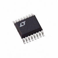
LTC1417ACGN Linear Technology, LTC1417ACGN Datasheet - Page 5

LTC1417ACGN
Manufacturer Part Number
LTC1417ACGN
Description
IC A/D CONV 14BIT SAMPLNG 16SSOP
Manufacturer
Linear Technology
Datasheet
1.LTC1417CGNPBF.pdf
(32 pages)
Specifications of LTC1417ACGN
Number Of Bits
14
Sampling Rate (per Second)
400k
Data Interface
MICROWIRE™, Serial, SPI™
Number Of Converters
1
Power Dissipation (max)
27.5mW Unipolar; 44mW Bipolar
Voltage Supply Source
Dual ±
Operating Temperature
0°C ~ 70°C
Mounting Type
Surface Mount
Package / Case
16-SSOP (0.150", 3.90mm Width)
Lead Free Status / RoHS Status
Contains lead / RoHS non-compliant
Available stocks
Company
Part Number
Manufacturer
Quantity
Price
Company:
Part Number:
LTC1417ACGN
Manufacturer:
LT
Quantity:
10 000
Part Number:
LTC1417ACGN
Manufacturer:
LTNEAR
Quantity:
20 000
Company:
Part Number:
LTC1417ACGN#PBF
Manufacturer:
CYPRESS
Quantity:
120
Part Number:
LTC1417ACGN#PBF
Manufacturer:
LINEAR/凌特
Quantity:
20 000
Company:
Part Number:
LTC1417ACGN#TRPBF
Manufacturer:
LT
Quantity:
450
TI I G CHARACTERISTICS
range, otherwise specifications are at T
TYPICAL PERFOR A CE CHARACTERISTICS
SYMBOL
t
t
t
t
f
Note 1: Absolute Maximum Ratings are those values beyond which the life
of a device may be impaired.
Note 2: All voltage values are with respect to ground with DGND and
AGND wired together (unless otherwise noted).
Note 3: When these pin voltages are taken below V
will be clamped by internal diodes. This product can handle input currents
greater than 100mA without latchup if the pin is driven below V
for unipolar mode) or above V
Note 4: When these pin voltages are taken below V
by internal diodes. This product can handle input currents greater than
100mA below V
Note 5: V
otherwise specified.
Note 6: Linearity, offset and full-scale specifications apply for a single-
ended A
H SCLK
L SCLK
H EXTCLKIN
L EXTCLKIN
CLKOUT
–0.5
–1.0
W
1.0
0.5
0
0
Typical INL Curve
IN
DD
U
+
input with A
= 5V, V
4096
SS
PARAMETER
SCLK High Time
SCLK Low Time
EXTCLKIN High Time
EXTCLKIN Low Time
Conversion Clock Output Frequency
without latchup. These pins are not clamped to V
SS
OUTPUT CODE
= – 5V, f
IN
8192
–
grounded.
DD
SAMPLE
.
12288
W
= 400kHz, t
U
16384
1417 G01
A
= 25 C. (Note 5)
r
SS
SS
= t
or above V
they will be clamped
f
= 5ns unless
– 0.5
–1.0
1.0
0.5
0
The
0
Differential Nonlinearity
vs Output Code
SS
CONDITIONS
(Note 9)
(Note 9)
Internal Conversion
Clock Mode (EXTCLKIN = 5V)
External Conversion Clock Mode
(EXTCLKIN is Driven by an External
Conversion Clock Input)
DD
(ground
indicates specifications which apply over the full operating temperature
, they
DD
4096
.
OUTPUT CODE
8192
Note 7: Integral nonlinearity is defined as the deviation of a code from a
straight line passing through the actual endpoints of the transfer curve.
The deviation is measured from the center of the quantization band.
Note 8: Bipolar offset is the offset voltage measured from – 0.5LSB
when the output code flickers between 0000 0000 0000 00 and
1111 1111 1111 11.
Note 9: Guaranteed by design, not subject to test.
Note 10: Recommended operating conditions.
Note 11: The falling CONVST edge starts a conversion. If CONVST returns
high at a critical point during the conversion it can create small errors. For
best results ensure that CONVST returns high either within 625ns after
conversion start or after BUSY rises.
Note 12: Typical RMS noise at the code transitions. See Figure 2 for
histogram.
Note 13: t
capture with 50% duty cycle. f
5ns setup time.
12288
11
of 40ns maximum allows f
(T
1417 G02
A
16384
= 25 C, unless otherwise specified)
SCLK
90
80
70
60
50
40
30
20
10
MIN
0.04
0.04
0
10
10
1k
S/(N + D) vs Input Frequency
and Amplitude
up to 20MHz for falling capture with
V
V
V
IN
IN
IN
SCLK
= –20dB
= 0dB
= –60dB
f
EXTCLKIN
INPUT FREQUENCY (Hz)
TYP
up to 10MHz for rising
9.4
10k
LTC1417
MAX
20
20
100k
sn1417 1417fas
UNITS
1417 G03
5
MHz
MHz
ns
ns
1M
s
s


