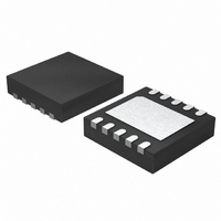
LTC2484CDD#PBF Linear Technology, LTC2484CDD#PBF Datasheet - Page 36

LTC2484CDD#PBF
Manufacturer Part Number
LTC2484CDD#PBF
Description
IC ADC 24BIT 10-DFN
Manufacturer
Linear Technology
Datasheet
1.LTC2484CDDTRPBF.pdf
(42 pages)
Specifications of LTC2484CDD#PBF
Number Of Bits
24
Sampling Rate (per Second)
6.8
Data Interface
MICROWIRE™, Serial, SPI™
Number Of Converters
1
Power Dissipation (max)
480µW
Voltage Supply Source
Single Supply
Operating Temperature
0°C ~ 70°C
Mounting Type
Surface Mount
Package / Case
10-WFDFN Exposed Pad
Number Of Elements
1
Resolution
24Bit
Architecture
Delta-Sigma
Sample Rate
0.0075KSPS
Input Polarity
Bipolar
Input Type
Voltage
Rated Input Volt
±2.75V
Differential Input
Yes
Power Supply Requirement
Single
Single Supply Voltage (typ)
3.3/5V
Single Supply Voltage (min)
2.7V
Single Supply Voltage (max)
5.5V
Dual Supply Voltage (typ)
Not RequiredV
Dual Supply Voltage (min)
Not RequiredV
Dual Supply Voltage (max)
Not RequiredV
Integral Nonlinearity Error
10ppm of Vref
Operating Temp Range
0C to 70C
Operating Temperature Classification
Commercial
Mounting
Surface Mount
Pin Count
10
Package Type
DFN EP
Input Signal Type
Differential
Lead Free Status / RoHS Status
Lead free / RoHS Compliant
Available stocks
Company
Part Number
Manufacturer
Quantity
Price
LTC2484
APPLICATIONS INFORMATION
be considered (see Input Current section). In this case,
the differential input current cancellation feature of the
LTC2484 allows external RC networks without signifi cant
degradation in DC performance.
Traditional high order delta-sigma modulators, while
providing very good linearity and resolution, suffer
from potential instabilities at large input signal levels.
The proprietary architecture used for the LTC2484 third
order modulator resolves this problem and guarantees
a predictable stable behavior at input signal levels of up
to 150% of full-scale. In many industrial applications,
it is not uncommon to have to measure microvolt level
signals superimposed over volt level perturbations and
the LTC2484 is eminently suited for such tasks. When the
perturbation is differential, the specifi cation of interest is
36
Figure 38. Measured Input Normal Mode Rejection vs Input Freq-
uency with Input Perturbation of 150% Full-Scale (50Hz Notch)
Figure 37. Measured Input Normal Mode Rejection vs Input Freq-
uency with Input Perturbation of 150% Full-Scale (60Hz Notch)
–100
–120
–100
–120
–20
–40
–60
–80
–20
–40
–60
–80
0
0
0
0
12.5 25 37.5 50 62.5 75 87.5 100 112.5 125 137.5 150 162.5 175 187.5
15
30
45
60
75
90
INPUT FREQUENCY (Hz)
INPUT FREQUENCY (Hz)
105 120 135 150 165 180 195 210 225
the normal mode rejection for large input signal levels. With
a reference voltage V
differential input range of 5V peak-to-peak. Figures 37 and
38 show measurement results for the LTC2484 normal
mode rejection ratio with a 7.5V peak-to-peak (150% of
full-scale) input signal superimposed over the more tradi-
tional normal mode rejection ratio results obtained with a
5V peak-to-peak (full-scale) input signal. In Figure 37, the
LTC2484 uses the internal oscillator with the notch set
at 60Hz (f
oscillator with the notch set at 50Hz. It is clear that the
LTC2484 rejection performance is maintained with no
compromises in this extreme situation. When operating
with large input signal levels, the user must observe that
such signals do not violate the device absolute maximum
ratings.
V
V
(150% OF FULL SCALE)
V
V
(150% OF FULL SCALE)
IN(P-P)
IN(P-P)
IN(P-P)
IN(P-P)
= 5V
= 7.5V
= 5V
= 7.5V
O
= LOW) and in Figure 38 it uses the internal
V
V
V
T
V
V
V
T
CC
REF
IN(CM)
A
CC
REF
INCM
A
= 25°C
REF
= 25°C
= 5V
= 5V
= 5V
= 5V
= 2.5
= 2.5
= 5V, the LTC2484 has a full-scale
2
2
2484fc


