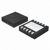
LTC2484CDD#PBF Linear Technology, LTC2484CDD#PBF Datasheet - Page 27

LTC2484CDD#PBF
Manufacturer Part Number
LTC2484CDD#PBF
Description
IC ADC 24BIT 10-DFN
Manufacturer
Linear Technology
Datasheet
1.LTC2484CDDTRPBF.pdf
(42 pages)
Specifications of LTC2484CDD#PBF
Number Of Bits
24
Sampling Rate (per Second)
6.8
Data Interface
MICROWIRE™, Serial, SPI™
Number Of Converters
1
Power Dissipation (max)
480µW
Voltage Supply Source
Single Supply
Operating Temperature
0°C ~ 70°C
Mounting Type
Surface Mount
Package / Case
10-WFDFN Exposed Pad
Number Of Elements
1
Resolution
24Bit
Architecture
Delta-Sigma
Sample Rate
0.0075KSPS
Input Polarity
Bipolar
Input Type
Voltage
Rated Input Volt
±2.75V
Differential Input
Yes
Power Supply Requirement
Single
Single Supply Voltage (typ)
3.3/5V
Single Supply Voltage (min)
2.7V
Single Supply Voltage (max)
5.5V
Dual Supply Voltage (typ)
Not RequiredV
Dual Supply Voltage (min)
Not RequiredV
Dual Supply Voltage (max)
Not RequiredV
Integral Nonlinearity Error
10ppm of Vref
Operating Temp Range
0C to 70C
Operating Temperature Classification
Commercial
Mounting
Surface Mount
Pin Count
10
Package Type
DFN EP
Input Signal Type
Differential
Lead Free Status / RoHS Status
Lead free / RoHS Compliant
Available stocks
Company
Part Number
Manufacturer
Quantity
Price
APPLICATIONS INFORMATION
rithm that forces the average differential input current to
zero independent of external settling errors. This allows
accurate direct digitization of high impedance sensors
without the need for buffers. Additional errors resulting
from mismatched leakage currents must also be taken
into account.
The switching algorithm forces the average input current
on the positive input (I
current on the negative input (I
conversion cycle, the average differential input current
(I
is zero, the common mode input current (I
proportional to the difference between the common mode
input voltage (V
voltage (V
In applications where the input common mode voltage
is equal to the reference common mode voltage, as in
the case of a balance bridge type application, both the
differential and common mode input current are zero.
The accuracy of the converter is unaffected by settling
errors. Mismatches in source impedances between IN
and IN
In applications where the input common mode voltage is
constant but different from the reference common mode
voltage, the differential input current remains zero while
the common mode input current is proportional to the
difference between V
common mode of 2.5V and an input common mode of
1.5V, the common mode input current is approximately
0.74μA (in simultaneous 50Hz/60Hz rejection mode). This
common mode input current has no effect on the accuracy
if the external source impedances tied to IN
matched. Mismatches in these source impedances lead to
a fi xed offset error but do not affect the linearity or full-
scale reading. A 1% mismatch in 1k source resistances
leads to a 15ppm shift (74μV) in offset voltage.
In applications where the common mode input voltage
varies as a function of input signal level (single-ended
input, RTDs, half bridges, current sensors, etc.), the
common mode input current varies proportionally with
IN
+
– I
–
also do not affect the accuracy.
IN
REFCM
–
) is zero. While the differential input current
INCM
).
) and the common mode reference
INCM
IN
+
) to be equal to the average input
and V
IN
REFCM
–
). Over the complete
. For a reference
IN
+
+
and IN
+ I
IN
–
)/2 is
–
are
+
input voltage. For the case of balanced input impedances,
the common mode input current effects are rejected by
the large CMRR of the LTC2484 leading to little degrada-
tion in accuracy. Mismatches in source impedances lead
to gain errors proportional to the difference between the
common mode input voltage and the common mode ref-
erence voltage. 1% mismatches in 1k source resistances
lead to gain worst-case gain errors on the order of 15ppm
(for 1V differences in reference and input common mode
voltage). Table 6 summarizes the effects of mismatched
source impedance and differences in reference/input
common mode voltages.
Table 6. Suggested Input Confi guration for LTC2484
Constant
V
Varying
V
The magnitude of the dynamic input current depends upon
the size of the very stable internal sampling capacitors and
upon the accuracy of the converter sampling clock. The
accuracy of the internal clock over the entire temperature
and power supply range is typically better than 0.5%. Such
a specifi cation can also be easily achieved by an external
clock. When relatively stable resistors (50ppm/°C) are
used for the external source impedance seen by IN
IN
will be insignifi cant (about 1% of their respective values
over the entire temperature and voltage range). Even for
the most stringent applications, a one-time calibration
operation may be suffi cient.
In addition to the input sampling charge, the input ESD
protection diodes have a temperature dependent leakage
current. This current, nominally 1nA (±10nA max), results
in a small offset shift. A 1k source resistance will create a
1μV typical and 10μV maximum offset voltage.
IN(CM)
IN(CM)
–
, the expected drift of the dynamic current and offset
– V
– V
REF(CM)
REF(CM)
BALANCED INPUT
RESISTANCES
C
IN
Large Source Resistance
with Negligible Error
C
and IN
Source Resistance with
Negligible Error
IN
IN
+
> 1nF at Both
> 1nF at Both IN
and IN
–
. Can Take Large
–
. Can Take
+
UNBALANCED INPUT
RESISTANCES
C
and IN
Source Resistance.
Unbalanced Resistance
Results in an Offset
Which Can Be Calibrated
Minimize IN
Capacitors and Avoid
Large Source Impedance
(<5k Recommended)
IN
LTC2484
> 1nF at Both IN
–
. Can Take Large
+
and IN
27
+
+
–
2484fc
and


