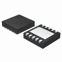
LTC2484CDD#PBF Linear Technology, LTC2484CDD#PBF Datasheet - Page 10

LTC2484CDD#PBF
Manufacturer Part Number
LTC2484CDD#PBF
Description
IC ADC 24BIT 10-DFN
Manufacturer
Linear Technology
Datasheet
1.LTC2484CDDTRPBF.pdf
(42 pages)
Specifications of LTC2484CDD#PBF
Number Of Bits
24
Sampling Rate (per Second)
6.8
Data Interface
MICROWIRE™, Serial, SPI™
Number Of Converters
1
Power Dissipation (max)
480µW
Voltage Supply Source
Single Supply
Operating Temperature
0°C ~ 70°C
Mounting Type
Surface Mount
Package / Case
10-WFDFN Exposed Pad
Number Of Elements
1
Resolution
24Bit
Architecture
Delta-Sigma
Sample Rate
0.0075KSPS
Input Polarity
Bipolar
Input Type
Voltage
Rated Input Volt
±2.75V
Differential Input
Yes
Power Supply Requirement
Single
Single Supply Voltage (typ)
3.3/5V
Single Supply Voltage (min)
2.7V
Single Supply Voltage (max)
5.5V
Dual Supply Voltage (typ)
Not RequiredV
Dual Supply Voltage (min)
Not RequiredV
Dual Supply Voltage (max)
Not RequiredV
Integral Nonlinearity Error
10ppm of Vref
Operating Temp Range
0C to 70C
Operating Temperature Classification
Commercial
Mounting
Surface Mount
Pin Count
10
Package Type
DFN EP
Input Signal Type
Differential
Lead Free Status / RoHS Status
Lead free / RoHS Compliant
Available stocks
Company
Part Number
Manufacturer
Quantity
Price
LTC2484
SDI (Pin 1): Serial Data Input. This pin is used to select
the line frequency rejection, input, temperature sensor
and 2x speed mode. Data is shifted into the SDI pin on
the rising edge of serial clock (SCK).
V
(Pin 8) with a 1μF tantalum capacitor in parallel with 0.1μF
ceramic capacitor as close to the part as possible.
TYPICAL PERFORMANCE CHARACTERISTICS
PIN FUNCTIONS
10
CC
250
200
150
100
50
(Pin 2): Positive Supply Voltage. Bypass to GND
0
2
Offset Error vs V
(2x Speed Mode)
V
V
V
f
T
O
A
REF
IN
IN(CM)
= GND
= 25°C
= 0V
2.5
= 2.5V
= GND
3
–100
–140
–120
–20
–40
–60
–80
3.5
V
0
CC
0
CC
PSRR vs Frequency at V
(2x Speed Mode)
(V)
V
REF
REF
IN
IN
f
T
O
CC
A
4
+
–
20
= GND
= 25°C
+
–
= GND
= GND
= 4.1V DC ±1.4V
= 2.5V
= GND
40 60
4.5
FREQUENCY AT V
80
5
2484 G36
100
5.5
120
140
CC
(Hz)
160
CC
200
240
230
220
210
190
180
170
160
180
0
Offset Error vs V
(2x Speed Mode)
200
V
V
V
f
T
2484 G39
O
CC
IN
IN(CM)
A
= GND
= 25°C
220
= 0V
= 5V
1
= GND
2
V
REF
V
this pin can have any value between 0.1V and V
negative reference input is GND (Pin 8).
IN
age on these pins can have any value between GND – 0.3V
and V
input range (V
REF
(V)
REF
+
3
(Pin 4), IN
(Pin 3): Positive Reference Input. The voltage on
CC
–120
–140
–100
–20
–60
–40
–80
+ 0.3V. Within these limits the converter bipolar
4
30600
0
PSRR vs Frequency at V
(2x Speed Mode)
2484 G37
V
REF
REF
IN
IN
f
T
O
A
CC
+
–
–
= GND
= 25°C
IN
+
–
= GND
= GND
= 4.1V DC ±0.7V
(Pin 5): Differential Analog Inputs. The volt-
5
= 2.5V
= GND
30650
= IN
FREQUENCY AT V
+
–100
–120
–140
–20
–40
–60
–80
– IN
0
30700
1
PSRR vs Frequency at V
(2x Speed Mode)
V
REF
REF
IN
IN
f
T
–
O
A
CC
) extends from –0.5 • V
+
–
= GND
= 25°C
+
–
= GND
= GND
= 4.1V DC
10
CC
= 2.5V
= GND
(Hz)
30750
FREQUENCY AT V
CC
100
2484 G40
30800
1k
CC
10k
(Hz)
CC
100k
CC
REF
. The
2484 G38
2484fc
1M
to


