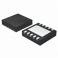
LTC2484CDD#PBF Linear Technology, LTC2484CDD#PBF Datasheet - Page 14

LTC2484CDD#PBF
Manufacturer Part Number
LTC2484CDD#PBF
Description
IC ADC 24BIT 10-DFN
Manufacturer
Linear Technology
Datasheet
1.LTC2484CDDTRPBF.pdf
(42 pages)
Specifications of LTC2484CDD#PBF
Number Of Bits
24
Sampling Rate (per Second)
6.8
Data Interface
MICROWIRE™, Serial, SPI™
Number Of Converters
1
Power Dissipation (max)
480µW
Voltage Supply Source
Single Supply
Operating Temperature
0°C ~ 70°C
Mounting Type
Surface Mount
Package / Case
10-WFDFN Exposed Pad
Number Of Elements
1
Resolution
24Bit
Architecture
Delta-Sigma
Sample Rate
0.0075KSPS
Input Polarity
Bipolar
Input Type
Voltage
Rated Input Volt
±2.75V
Differential Input
Yes
Power Supply Requirement
Single
Single Supply Voltage (typ)
3.3/5V
Single Supply Voltage (min)
2.7V
Single Supply Voltage (max)
5.5V
Dual Supply Voltage (typ)
Not RequiredV
Dual Supply Voltage (min)
Not RequiredV
Dual Supply Voltage (max)
Not RequiredV
Integral Nonlinearity Error
10ppm of Vref
Operating Temp Range
0C to 70C
Operating Temperature Classification
Commercial
Mounting
Surface Mount
Pin Count
10
Package Type
DFN EP
Input Signal Type
Differential
Lead Free Status / RoHS Status
Lead free / RoHS Compliant
Available stocks
Company
Part Number
Manufacturer
Quantity
Price
APPLICATIONS INFORMATION
LTC2484
Through timing control of the CS and SCK pins, the LTC2484
offers several fl exible modes of operation (internal or
external SCK and free-running conversion modes). These
various modes do not require programming confi guration
registers; moreover, they do not disturb the cyclic operation
described above. These modes of operation are described
in detail in the Serial Interface Timing Modes section.
Easy Drive Input Current Cancellation
The LTC2484 combines a high precision delta-sigma ADC
with an automatic differential input current cancellation
front end. A proprietary front-end passive sampling
network transparently removes the differential input
current. This enables external RC networks and high
impedance sensors to directly interface to the LTC2484
without external amplifi ers. The remaining common
mode input current is eliminated by either balancing the
differential input impedances or setting the common
mode input equal to the common mode reference (see
Automatic Input Current Cancellation section). This unique
architecture does not require on-chip buffers enabling
input signals to swing all the way to ground and up to
V
the transparent offset and full-scale autocalibration and
the absolute accuracy (full-scale + offset + linearity) is
maintained with external RC networks.
Accessing the Special Features of the LTC2484
The LTC2484 combines a high resolution, low noise ΔΣ
analog-to-digital converter with an on-chip selectable
temperature sensor, programmable digital fi lter and output
rate control. These special features are selected through a
14
CC
. Furthermore, the cancellation does not interfere with
Table 1. Selecting Special Modes
EN
0
1
1
1
1
1
1
1
1
1
1
IM FoA FoB SPD
X
0
0
0
0
0
0
1
1
1
X
X
0
0
1
0
0
1
0
0
1
1
X
0
1
0
0
1
0
0
1
0
1
2484 TBL1
X
X
X
X
X
0
0
0
1
1
1
Comments
Keep Previous Mode
External Input, 50Hz and 60Hz Rejection, Autocalibration
External Input, 50Hz Rejection, Autocalibration
External Input, 60Hz Rejection, Autocalibration
External Input, 50Hz and 60Hz Rejection, 2x Speed
External Input, 50Hz Rejection, 2x Speed
External Input, 60Hz Rejection, 2x Speed
Temperature Input, 50Hz and 60Hz Rejection, Autocalibration
Temperature Input, 50Hz Rejection, Autocalibration
Temperature Input, 60Hz Rejection, Autocalibration
Reserved, Do Not Use
single 8-bit serial input word during the data input/output
cycle (see Figure 2).
The LTC2484 powers up in a default mode commonly used
for most measurements. The device will remain in this
mode as long as the serial data input (SDI) is low. In this
default mode, the measured input is external, the digital
fi lter simultaneously rejects 50Hz and 60Hz line frequency
noise, and the speed mode is 1x (offset automatically,
continuously calibrated).
A simple serial interface grants access to any or all special
functions contained within the LTC2484. In order to change
the mode of operation, an enable bit (EN) followed by up
to 7 bits of data are shifted into the device (see Table 1).
The fi rst 3 bits, in order to remain pin-compatible with the
LTC2480, are don’t-cares and can be either HIGH or LOW.
The 4th bit (IM) is used to select the internal temperature
sensor as the conversion input, while the 5th and 6th bits
(FA, FB) combine to determine the line frequency rejection
mode. The 7th bit (SPD) is used to double the output rate
by disabling the offset auto calibration.
Temperature Sensor (IM)
The LTC2484 includes an on-chip temperature sensor.
The temperature sensor is selected by setting IM = 1 in
the serial input data stream. Conversions are performed
directly on the temperature sensor by the converter. While
operating in this mode, the device behaves as a temperature
to bits converter. The digital reading is proportional to the
absolute temperature of the device. This feature allows
the converter to linearize temperature sensors or continu-
ously remove temperature effects from external sensors.
2484fc


