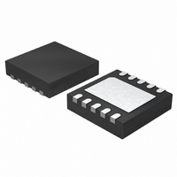
LTC2484CDD#PBF Linear Technology, LTC2484CDD#PBF Datasheet - Page 32

LTC2484CDD#PBF
Manufacturer Part Number
LTC2484CDD#PBF
Description
IC ADC 24BIT 10-DFN
Manufacturer
Linear Technology
Datasheet
1.LTC2484CDDTRPBF.pdf
(42 pages)
Specifications of LTC2484CDD#PBF
Number Of Bits
24
Sampling Rate (per Second)
6.8
Data Interface
MICROWIRE™, Serial, SPI™
Number Of Converters
1
Power Dissipation (max)
480µW
Voltage Supply Source
Single Supply
Operating Temperature
0°C ~ 70°C
Mounting Type
Surface Mount
Package / Case
10-WFDFN Exposed Pad
Number Of Elements
1
Resolution
24Bit
Architecture
Delta-Sigma
Sample Rate
0.0075KSPS
Input Polarity
Bipolar
Input Type
Voltage
Rated Input Volt
±2.75V
Differential Input
Yes
Power Supply Requirement
Single
Single Supply Voltage (typ)
3.3/5V
Single Supply Voltage (min)
2.7V
Single Supply Voltage (max)
5.5V
Dual Supply Voltage (typ)
Not RequiredV
Dual Supply Voltage (min)
Not RequiredV
Dual Supply Voltage (max)
Not RequiredV
Integral Nonlinearity Error
10ppm of Vref
Operating Temp Range
0C to 70C
Operating Temperature Classification
Commercial
Mounting
Surface Mount
Pin Count
10
Package Type
DFN EP
Input Signal Type
Differential
Lead Free Status / RoHS Status
Lead free / RoHS Compliant
Available stocks
Company
Part Number
Manufacturer
Quantity
Price
LTC2484
APPLICATIONS INFORMATION
second, the user is advised to maximize the power supply
voltage used and to limit the maximum ambient operating
temperature. In certain circumstances, a reduction of the
differential reference voltage may be benefi cial.
Input Bandwidth
The combined effect of the internal SINC
of the analog and digital autocalibration circuits determines
the LTC2484 input bandwidth. When the internal oscillator
32
Figure 24. Resolution (INL
vs Output Data Rate and Temperature
–10
22
20
14
10
20
15
10
18
16
12
–5
0
5
Figure 25. Offset Error vs Output
Data Rate and Reference Voltage
0
0
V
V
f
T
V
V
f
RES = LOG 2 (V
O
O
IN(CM)
IN
A
IN(CM)
CC
10
10
= EXT CLOCK
= EXT CLOCK
= 25°C
OUTPUT DATA RATE (READINGS/SEC)
OUTPUT DATA RATE (READINGS/SEC)
= 0V
= V
T
A
20 30
20 30
REF
V
= V
= V
= 85°C
CC
REF(CM)
REF(CM)
= 5V
= 5V, V
REF
40
40
/INL
REF
V
50
50
CC
MAX
= 2.5V
= V
T
A
60
60
)
REF
= 25°C
70
70
RMS
= 5V
80
80
≤ 1LSB)
4
90 100
90 100
2484 F25
2484 F24
digital fi lter and
is used with the notch set at 60Hz, the 3dB input bandwidth
is 3.63Hz. When the internal oscillator is used with the
notch set at 50Hz, the 3dB input bandwidth is 3.02Hz. If
an external conversion clock generator of frequency f
is connected to the f
• 10
Due to the complex fi ltering and calibration algorithms
utilized, the converter input bandwidth is not modeled
very accurately by a fi rst order fi lter with the pole located
–6
• f
EOSC
Figure 26. Resolution (Noise
vs Output Data Rate and Reference Voltage
Figure 27. Resolution (INL
Output Data Rate and Reference Voltage
24
18
14
10
22
14
10
22
20
16
12
20
18
16
12
0
0
.
V
V
f
T
RES = LOG 2 (V
V
V
REF
f
T
RES = LOG 2 (V
V
V
O
O
A
A
IN(CM)
IN
IN(CM)
IN
CC
CC
= EXT CLOCK
10
10
= EXT CLOCK
= 25°C
= 25°C
OUTPUT DATA RATE (READINGS/SEC)
OUTPUT DATA RATE (READINGS/SEC)
= 0V
–
= 0V
= 5V, V
= 5V, V
= GND
20 30
20 30
= V
= V
O
pin, the 3dB input bandwidth is 11.8
REF(CM)
REF(CM)
REF
REF
REF
= 2.5V
= 2.5V
REF
40
40
/NOISE
/INL
50
50
MAX
V
V
CC
60
60
RMS
CC
)
= V
= V
RMS
)
70
70
REF
REF
RMS
80
80
= 5V
≤ 1LSB) vs
= 5V
≤ 1LSB)
90 100
90 100
2484 F26
2484 F27
EOSC
2484fc


