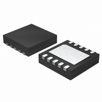
LTC2484CDD#PBF Linear Technology, LTC2484CDD#PBF Datasheet - Page 13

LTC2484CDD#PBF
Manufacturer Part Number
LTC2484CDD#PBF
Description
IC ADC 24BIT 10-DFN
Manufacturer
Linear Technology
Datasheet
1.LTC2484CDDTRPBF.pdf
(42 pages)
Specifications of LTC2484CDD#PBF
Number Of Bits
24
Sampling Rate (per Second)
6.8
Data Interface
MICROWIRE™, Serial, SPI™
Number Of Converters
1
Power Dissipation (max)
480µW
Voltage Supply Source
Single Supply
Operating Temperature
0°C ~ 70°C
Mounting Type
Surface Mount
Package / Case
10-WFDFN Exposed Pad
Number Of Elements
1
Resolution
24Bit
Architecture
Delta-Sigma
Sample Rate
0.0075KSPS
Input Polarity
Bipolar
Input Type
Voltage
Rated Input Volt
±2.75V
Differential Input
Yes
Power Supply Requirement
Single
Single Supply Voltage (typ)
3.3/5V
Single Supply Voltage (min)
2.7V
Single Supply Voltage (max)
5.5V
Dual Supply Voltage (typ)
Not RequiredV
Dual Supply Voltage (min)
Not RequiredV
Dual Supply Voltage (max)
Not RequiredV
Integral Nonlinearity Error
10ppm of Vref
Operating Temp Range
0C to 70C
Operating Temperature Classification
Commercial
Mounting
Surface Mount
Pin Count
10
Package Type
DFN EP
Input Signal Type
Differential
Lead Free Status / RoHS Status
Lead free / RoHS Compliant
Available stocks
Company
Part Number
Manufacturer
Quantity
Price
APPLICATIONS INFORMATION
CONVERTER OPERATION
Converter Operation Cycle
The LTC2484 is a low power, delta-sigma analog-to-digital
converter with an easy to use 4-wire serial interface
and automatic differential input current cancellation.
Its operation is made up of three states. The converter
operating cycle begins with the conversion, followed by
the low power sleep state and ends with the data output
(see Figure 1). The 4-wire interface consists of serial data
output (SDO), serial clock (SCK), chip select (CS) and
serial data input (SDI).
Initially, the LTC2484 performs a conversion. Once the
conversion is complete, the device enters the sleep state.
SDO
SCK
SDI
CS
SLEEP
Figure 1. LTC2484 State Transition Diagram
Hi-Z
BIT 31
EOC
EN
FALSE
CONFIGURATION INPUT
BIT 30
DMY
DATA OUTPUT
DON’T CARE
CONVERT
CS = LOW
SCK
SLEEP
AND
BIT 29
SIG
TRUE
2484 F01
BIT 28
MSB
BIT 27 BIT 26
IM
Figure 2. Input/Output Data Timing
FOA
CONVERSION RESULT
FOB
DATA INPUT/OUTPUT
SPD
While in this sleep state, power consumption is
reduced by two orders of magnitude. The part re-
mains in the sleep state as long as CS is HIGH. The
conversion result is held indefi nitely in a static shift
register while the converter is in the sleep state.
Once CS is pulled LOW, the device exits the low
power mode and enters the data output state. If CS
is pulled HIGH before the fi rst rising edge of SCK,
the device returns to the low power sleep mode
and the conversion result is still held in the internal
static shift register. If CS remains LOW after the
fi rst rising edge of SCK, the device begins output-
ting the conversion result. Taking CS HIGH at this
point will terminate the data input and output state
and start a new conversion. The conversion result
is shifted out of the device through the serial data
output pin (SDO) on the falling edge of the serial
clock (SCK) (see Figure 2). The LTC2484 includes a
serial data input pin (SDI) in which data is latched
by the device on the rising edge of SCK (Figure 2).
The bit stream applied to this pin can be used to
select various features of the LTC2484, including an
on-chip temperature sensor, line frequency rejection
and output data rate. Alternatively, this pin may be
tied to ground and the part will perform conversions
in a default state. In the default state (SDI grounded)
the device simply performs conversions on the user
applied input with simultaneous rejection of 50Hz
and 60Hz line frequencies.
LSB24
BIT 5
BIT 4
BIT 3
SUB LSBs
DON’T CARE
BIT 2
BIT 1
BIT 0
LTC2484
CONVERSION
2484 F02
13
2484fc


