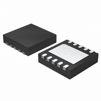
LTC2484CDD#PBF Linear Technology, LTC2484CDD#PBF Datasheet - Page 31

LTC2484CDD#PBF
Manufacturer Part Number
LTC2484CDD#PBF
Description
IC ADC 24BIT 10-DFN
Manufacturer
Linear Technology
Datasheet
1.LTC2484CDDTRPBF.pdf
(42 pages)
Specifications of LTC2484CDD#PBF
Number Of Bits
24
Sampling Rate (per Second)
6.8
Data Interface
MICROWIRE™, Serial, SPI™
Number Of Converters
1
Power Dissipation (max)
480µW
Voltage Supply Source
Single Supply
Operating Temperature
0°C ~ 70°C
Mounting Type
Surface Mount
Package / Case
10-WFDFN Exposed Pad
Number Of Elements
1
Resolution
24Bit
Architecture
Delta-Sigma
Sample Rate
0.0075KSPS
Input Polarity
Bipolar
Input Type
Voltage
Rated Input Volt
±2.75V
Differential Input
Yes
Power Supply Requirement
Single
Single Supply Voltage (typ)
3.3/5V
Single Supply Voltage (min)
2.7V
Single Supply Voltage (max)
5.5V
Dual Supply Voltage (typ)
Not RequiredV
Dual Supply Voltage (min)
Not RequiredV
Dual Supply Voltage (max)
Not RequiredV
Integral Nonlinearity Error
10ppm of Vref
Operating Temp Range
0C to 70C
Operating Temperature Classification
Commercial
Mounting
Surface Mount
Pin Count
10
Package Type
DFN EP
Input Signal Type
Differential
Lead Free Status / RoHS Status
Lead free / RoHS Compliant
Available stocks
Company
Part Number
Manufacturer
Quantity
Price
APPLICATIONS INFORMATION
through the input and the reference pins. If large external
input and/or reference capacitors (C
previous section provides formulae for evaluating the effect
of the source resistance upon the converter performance for
any value of f
capacitors (C
source resistance upon the LTC2484 typical performance
can be inferred from Figures 13, 14, 15 and 16 in which
the horizontal axis is scaled by 307200/f
Figure 20. Offset Error vs Output Data Rate and Temperature
Figure 22. –FS Error vs Output Data Rate and Temperature
–1000
–1500
–2000
–2500
–3500
–3000
–500
–10
50
40
30
20
10
0
0
EOSC
IN
0
0
V
V
V
f
V
V
f
, C
O
O
IN(CM)
CC
IN
IN(CM)
CC
10
10
= EXT CLOCK
= EXT CLOCK
OUTPUT DATA RATE (READINGS/SEC)
OUTPUT DATA RATE (READINGS/SEC)
= 0V
. If small external input and/or reference
= V
REF
= V
20
20 30
REF
REF
= V
= V
) are used, the effect of the external
REF(CM)
= 5V
30
REF(CM)
= 5V
T
T
T
A
40
A
40
A
= 85°C
= 85°C
= 25°C
50
50
60
60
T
A
70
70
= 25°C
IN
80
80
, C
REF
90
90 100
2484 F20
2484 F22
EOSC
100
) are used, the
.
Third, an increase in the frequency of the external oscillator
above 1MHz (a more than 3× increase in the output data
rate) will start to decrease the effectiveness of the internal
autocalibration circuits. This will result in a progressive
degradation in the converter accuracy and linearity. Typical
measured performance curves for output data rates up to
100 readings per second are shown in Figures 20 to 27. In
order to obtain the highest possible level of accuracy from
this converter at output data rates above 20 readings per
Figure 21. +FS Error vs Output Data Rate and Temperature
3500
3000
2000
1000
Figure 23. Resolution (Noise
vs Output Data Rate and Temperature
2500
1500
500
24
22
20
18
16
14
12
10
0
0
0
V
V
f
V
V
V
f
RES = LOG 2 (V
O
O
IN(CM)
CC
IN(CM)
CC
IN
10
10
= EXT CLOCK
OUTPUT DATA RATE (READINGS/SEC)
= EXT CLOCK
OUTPUT DATA RATE (READINGS/SEC)
= V
= 0V
= V
T
A
20 30
20 30
REF
= V
= 85°C
REF
= V
REF(CM)
= 5V
REF(CM)
= 5V
REF
T
40
40
A
= 85°C
/NOISE
50
50
T
A
60
60
RMS
= 25°C
70
70
T
)
A
RMS
= 25°C
80
80
≤ 1LSB)
LTC2484
90 100
90 100
2484 F21
2484 F23
31
2484fc


