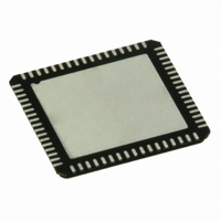
ADC16DV160CILQ/NOPB National Semiconductor, ADC16DV160CILQ/NOPB Datasheet - Page 9

ADC16DV160CILQ/NOPB
Manufacturer Part Number
ADC16DV160CILQ/NOPB
Description
ADC 16BIT DUAL 160MSPS 68LLP
Manufacturer
National Semiconductor
Series
PowerWise®r
Datasheet
1.ADC16DV160CILQNOPB.pdf
(30 pages)
Specifications of ADC16DV160CILQ/NOPB
Number Of Bits
16
Sampling Rate (per Second)
160M
Data Interface
Serial, SPI™
Number Of Converters
2
Power Dissipation (max)
1.47W
Voltage Supply Source
Single Supply
Operating Temperature
-40°C ~ 85°C
Mounting Type
Surface Mount
Package / Case
68-VFQFN, Exposed Pad
Leaded Process Compatible
Yes
Rohs Compliant
Yes
Peak Reflow Compatible (260 C)
Yes
Lead Free Status / RoHS Status
Lead free / RoHS Compliant
Other names
ADC16DV160CILQ
t
t
CSH
IAG
Note 1: Absolute Maximum Ratings indicate limits beyond which damage to the device may occur. Operating Ratings indicate conditions for which the device is
guaranteed to be functional, but do not guarantee specific performance limits. For guaranteed specifications and test conditions, see the Electrical Characteristics.
The guaranteed specifications apply only for the test conditions listed. Some performance characteristics may degrade when the device is not operated under
the listed test conditions. Operation of the device beyond the maximum Operating Ratings is not recommended.
Note 2: All voltages are measured with respect to GND = AGND = DRGND = 0V, unless otherwise specified.
Note 3: When the input voltage at any pin exceeds the power supplies (that is, V
±50 mA maximum package input current rating limits the number of pins that can safely exceed the power supplies with an input current of ±5mA to 10.
Note 4: Human Body Model is 100 pF discharged through a 1.5 kΩ resistor. Machine Model is 220 pF discharged through 0 Ω.
Note 5: Reflow temperature profiles are different for lead-free and non-lead-free packages.
Note 6: Typical figures are at T
guaranteed.
Note 7: The inputs are protected as shown below. Input voltage magnitudes above V
per
Note 8: The input capacitance is the sum of the package/pin capacitance and the sample and hold circuit capacitance.
Note 9: This parameter is specified in units of dBFS – dB relative to the ADC's input full-scale voltage.
Note 10: This parameter is a function of the CLK frequency - increasing directly as the frequency is lowered.
Note 11: This parameter is guaranteed only at 25°C. For power dissipation over temperature range, refer to Power vs. Temperature plot in Typical Performance
Characteristics, Dynamic Performance.
Timing Diagrams
Symbol
(Note
3). However, errors in the A/D conversion can occur if the input goes above 2.6V or below GND as described in the Operating Ratings section.
CSB Hold Time
Inter-access Gap
A
= 25°C and represent most likely parametric norms at the time of product characterization. The typical specifications are not
Parameter
FIGURE 1. Digital Output Timing
Minimum time CSB must be
deasserted between accesses
9
IN
< AGND, or V
A3.0
30101457
or below GND will not damage this device, provided current is limited
Conditions
IN
> V
A
), the current at that pin should be limited to ±5 mA. The
Typ
Max
30
5
www.national.com
30101403
ns (min)
ns (min)
Units


