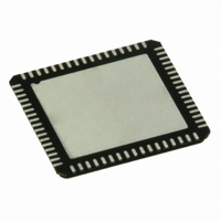
ADC16DV160CILQ/NOPB National Semiconductor, ADC16DV160CILQ/NOPB Datasheet - Page 17

ADC16DV160CILQ/NOPB
Manufacturer Part Number
ADC16DV160CILQ/NOPB
Description
ADC 16BIT DUAL 160MSPS 68LLP
Manufacturer
National Semiconductor
Series
PowerWise®r
Datasheet
1.ADC16DV160CILQNOPB.pdf
(30 pages)
Specifications of ADC16DV160CILQ/NOPB
Number Of Bits
16
Sampling Rate (per Second)
160M
Data Interface
Serial, SPI™
Number Of Converters
2
Power Dissipation (max)
1.47W
Voltage Supply Source
Single Supply
Operating Temperature
-40°C ~ 85°C
Mounting Type
Surface Mount
Package / Case
68-VFQFN, Exposed Pad
Leaded Process Compatible
Yes
Rohs Compliant
Yes
Peak Reflow Compatible (260 C)
Yes
Lead Free Status / RoHS Status
Lead free / RoHS Compliant
Other names
ADC16DV160CILQ
Input Common Mode
The analog inputs of the ADC16DV160 are not internally dc
biased and the range of input common mode is very narrow.
Hence it is highly recommended to use the common mode
voltage (V
timal dynamic performance regardless of DC and AC coupling
applications. Input common mode signal must be decoupled
with low ESL 0.1 μF input bias resistors to minimize noise
performance degradation due to any coupling or switching
noise between the ADC16DV160 and input driving circuit.
Transformers act as band pass filters. The lower frequency
limit is set by saturation at frequencies below a few MHz and
parasitic resistance and capacitance set the upper frequency
limit. The transformer core will be saturated with excessive
signal power and it causes distortion as the equivalent load
termination becomes heavier at high input frequencies. This
is a reason to reduce shunt capacitors for high IF sampling
applications to balance the amount of distortion caused by the
transformer and charge kick-back noise from the device.
As input frequency goes higher with the input network in
ure
positive and negative inputs (V
impedance mismatch between the two primary ports of the
transformer since one is connected to the signal source and
the other is connected to GND. Distortion increases as a re-
sult.
Equivalent Input Circuit and Its S11
The input circuit of the ADC16DV160 during sample mode is
a differential switched capacitor as shown in
bottom plate sampling switch is bootstrapped in order to re-
duce its turn on impedance and its variation across input
signal amplitude. Bottom plate sampling switches, and top
plate sampling switch are all turned off during hold mode. The
sampled analog input signal is processed through the follow-
5, amplitude and phase unbalance increase between
RM
, typically 1.15V) as input common mode for op-
IN+
FIGURE 6. Transformer Drive Circuit for High Input Frequency
FIGURE 5. Transformer Drive Circuit for Low Input Frequency
and V
IN-
) due to the inherent
Figure
7. The
Fig-
17
Driving Analog Inputs
For low frequency applications, either a flux or balun trans-
former can convert single-ended input signals into differential
and drive the ADC16DV160 without additive noise. An exam-
ple is shown in
common mode by connecting the center tap of the
transformer’s secondary ports. A flux transformer is used for
this example, but AC coupling capacitors enable the use of a
balun type transformer.
The cascaded transmission line (balun) transformers in
ure 6
sampling base station receive channels. The transmission
line transformer has less stray capacitance between primary
and secondary ports and so the impedance mismatch at the
secondary ports is effectively less even with the given inher-
ent impedance mismatch on the primary ports. Cascading two
transmission line transformers further reduces the effective
stray capacitance from the secondary ports of the secondary
transformer to primary ports of first transformer, where the
impedance is mismatched. A transmission line transformer,
for instance MABACT0040 from M/A-COM, with a center tap
on the secondary port can further reduce amplitude and
phase mismatch.
ing pipeline ADC core. The equivalent impedance changes
drastically between sample and hold mode and a significant
amount of charge injection occurs during the transition be-
tween the two operating modes.
Distortion and SNR heavily rely on the signal integrity,
impedance matching during sample mode and charge injec-
tion due to the sampling switches.
can be used for high frequency applications like high IF
Figure
5. The V
30101407
RM
pin is used to bias the input
30101408
www.national.com
Fig-


