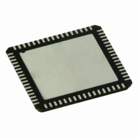
ADC16DV160CILQ/NOPB National Semiconductor, ADC16DV160CILQ/NOPB Datasheet - Page 19

ADC16DV160CILQ/NOPB
Manufacturer Part Number
ADC16DV160CILQ/NOPB
Description
ADC 16BIT DUAL 160MSPS 68LLP
Manufacturer
National Semiconductor
Series
PowerWise®r
Datasheet
1.ADC16DV160CILQNOPB.pdf
(30 pages)
Specifications of ADC16DV160CILQ/NOPB
Number Of Bits
16
Sampling Rate (per Second)
160M
Data Interface
Serial, SPI™
Number Of Converters
2
Power Dissipation (max)
1.47W
Voltage Supply Source
Single Supply
Operating Temperature
-40°C ~ 85°C
Mounting Type
Surface Mount
Package / Case
68-VFQFN, Exposed Pad
Leaded Process Compatible
Yes
Rohs Compliant
Yes
Peak Reflow Compatible (260 C)
Yes
Lead Free Status / RoHS Status
Lead free / RoHS Compliant
Other names
ADC16DV160CILQ
3.0 CLOCK INPUT CONSIDERATIONS
Clock Input Modes
The ADC16DV160 provides a low additive jitter differential
clock receiver for optimal dynamic performance over a wide
input frequency range. The input common mode of the clock
receiver is internally biased at V
as shown in
be AC-coupled. It is possible to DC-couple the clock input, but
the common mode (average voltage of CLK+ and CLK-) must
not be higher than V
reduction leading to lowered jitter performance. CLK+ and
CLK- should never be lower than AGND. A high speed back-
to-back diode connected between CLK+ and CLK- can limit
the maximum swing, but this could cause signal integrity con-
cerns when the diode turns on and reduces the load
impedance instantaneously.
The preferred differential transformer coupled clocking ap-
proach is shown in
on the center tap of the secondary of a flux type transformer
stabilizes clock input common mode. Differential clocking in-
creases the maximum amplitude of the clock input at the pins
6dB vs. the singled-ended circuit shown in
clock amplitude is recommended to be as large as possible
while CLK+ and CLK- both never exceed the supply rails of
V
ferential clock receiver shown in
amplitude at CLK+ and CLK- pins increases its slope around
the zero-crossing point so that higher signal-to-noise results.
The differential receiver of the ADC16DV160 has an extreme-
ly low-noise floor but its bandwidth is also extremely wide. The
wide band clock noise folds back into the first Nyquist zone at
the ADC output. Increased slope of the input clock lowers the
equivalent noise contributed by the differential receiver.
A band-pass filter (BPF) with narrow pass band and low in-
sertion loss can be added to the clock input signal path when
the wide band noise of the clock source is noticeably large
compared to the input equivalent noise of the differential clock
receiver.
Load termination can be a combination of R and C instead of
a pure R. This RC termination can improve the noise perfor-
mance of the clock signal path by filtering out high frequency
noise through a low pass filter. The size of R and C is depen-
dent on the clock rate and slope of the clock input.
A1.8
and AGND. With the equivalent input noise of the dif-
FIGURE 9. Equivalent Clock Receiver
Figure
9. Normally the external clock input should
Figure
A1.8
/2 to prevent substantial tail current
10. A 0.1 μF decoupling capacitor
A1.8
/2 through a 10 kΩ resistor
Figure
9, a larger clock
Figure
30101431
11. The
19
An LVPECL and/or LVDS driver can also drive the AD-
C16DV160. However the full dynamic performance of the
ADC16DV160 might not be achieved due to the high noise
floor of the driving circuit itself especially in high IF sampling
applications.
A singled-ended clock can drive the CLK+ pin through a 0.1
µF AC coupling capacitor while CLK- is decoupled to AGND
through a 0.1 μF capacitor as shown in
FIGURE 11. Singled-Ended 1.8V Clocking, Capacitive AC
Duty Cycle Stabilizer
The highest operating speed with optimal performance can
only be achieved with a 50% clock duty cycle because the
switched-capacitor circuit of the ADC16DV160 is designed to
have equal amount of settling time between each stage. The
maximum operating frequency could be reduced accordingly
when the clock duty cycle departs from 50%.
The ADC16DV160 contains a duty cycle stabilizer that ad-
justs the non-sampling (rising) clock edge to make the duty
cycle of the internal clock 50% for a 30-to-70% input clock
duty cycle. The duty cycle stabilizer is always on because the
noise and distortion performance are not affected at all. It is
not recommended to use the ADC16DV160 at clock frequen-
cies less than 20 MSPS where the feedback loop in the duty
cycle stabilizer becomes unstable.
Clock Jitter vs. Dynamic Performance
High speed and high resolution ADCs require a low-noise
clock input to ensure full dynamic performance over wide in-
put frequency range. SNR (SNR
(Fin) can be calculated by:
with a given total noise power (V
(Tj), and input amplitude (A) in dBFS.
The clock signal path must be treated as an analog signal
whenever aperture jitter affects the dynamic performance of
FIGURE 10. Differential Clocking, Transformer Coupled
Coupled
Fin
N
2
) at a given input frequency
) of an ADC, total rms jitter
Figure
11.
30101434
www.national.com
30101433
30101432


