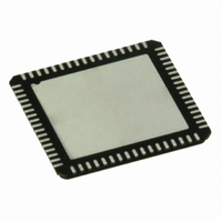
ADC16DV160CILQ/NOPB National Semiconductor, ADC16DV160CILQ/NOPB Datasheet - Page 4

ADC16DV160CILQ/NOPB
Manufacturer Part Number
ADC16DV160CILQ/NOPB
Description
ADC 16BIT DUAL 160MSPS 68LLP
Manufacturer
National Semiconductor
Series
PowerWise®r
Datasheet
1.ADC16DV160CILQNOPB.pdf
(30 pages)
Specifications of ADC16DV160CILQ/NOPB
Number Of Bits
16
Sampling Rate (per Second)
160M
Data Interface
Serial, SPI™
Number Of Converters
2
Power Dissipation (max)
1.47W
Voltage Supply Source
Single Supply
Operating Temperature
-40°C ~ 85°C
Mounting Type
Surface Mount
Package / Case
68-VFQFN, Exposed Pad
Leaded Process Compatible
Yes
Rohs Compliant
Yes
Peak Reflow Compatible (260 C)
Yes
Lead Free Status / RoHS Status
Lead free / RoHS Compliant
Other names
ADC16DV160CILQ
www.national.com
ANALOG I/O
DIGITAL I/O
Pin Descriptions
Pin(s)
10, 11
12, 13
7, 8
5, 6
66
20
67
19
16
26
25
23
24
27
2
9
Name
SCLK
CLK+
CLK−
SDIO
V
V
V
V
V
V
V
V
CSB
V
V
V
IN+Q
IN−Q
RPQ
RNQ
RMQ
REF
IN+I
IN−I
RMI
RPI
RNI
Output/Input
Input/Output
Output
Output
Output
Type
Input
Input
Input
Input
Input
Input
Function and Connection
Differential analog input pins. The differential full-scale input signal level
is 2.4 V
pin signal is centered on a common mode voltage, V
Upper reference voltage.
This pin should not be used to source or sink current. The decoupling
capacitor to AGND (low ESL 0.1 µF) should be placed very close to the
pin to minimize stray inductance. V
through a low ESL 0.1 µF and a low ESR 10 µF capacitors in parallel.
Lower reference voltage.
This pin should not be used to source or sink current. The decoupling
capacitor to AGND (low ESL 0.1 µF) should be placed very close to the
pin to minimize stray inductance. V
through a low ESL 0.1 µF and a low ESR 10 µF capacitors in parallel.
Common mode voltage
These pins should be bypassed to AGND with a low ESL (equivalent
series inductance) 0.1 µF capacitor placed as close to the pin as
possible to minimize stray inductance, and a 10 µF capacitor should be
placed in parallel. It is recommended to use V
mode voltage for the differential analog inputs.
Internal reference voltage output / External reference voltage input. By
default, this pin is the output for the internal 1.2V voltage reference. This
pin should not be used to sink or source current and should be
decoupled to AGND with a 0.1 µF, low ESL capacitor. The decoupling
capacitors should be placed as close to the pins as possible to minimize
inductance and optimize ADC performance. The decoupling capacitor
should not be larger than 0.1 µF, otherwise dynamic performance after
power-up calibration can decrease due to the extended V
time.
This pin can also be used as the input for a low noise external reference
voltage. The output impedance for the internal reference at this pin is
10kΩ and this can be overdriven provided the impedance of the external
source is < 10kΩ. Careful decoupling is just as essential when an
external reference is used. The 0.1 µF low ESL decoupling capacitor
should be placed as close to this pin as possible.
The default Input differential voltage swing is equal to 2 * V
this can be changed through the SPI.
Differential clock input pins. DC biasing is provided internally. For single-
ended clock mode, drive CLK+ through AC coupling while decoupling
CLK- pin to AGND.
Serial Clock. Serial data is shifted into and out of the device synchronous
with this clock signal.
Serial Data In/Out. Serial data is shifted into the device on this pin while
the CSB signal is asserted and data input mode is selected. Serial data
is shifted out of the device on this pin while CSB is asserted and data
output mode is selected.
Serial Chip Select. When this signal is asserted SCLK is used to clock
input or output serial data on the SDIO pin. When this signal is de-
asserted, the SDIO pin is a high impedence and the input data is
ignored.
4
PP
by default, but can be set to 2.4/2.0 V
RP
RN
needs to be connected to V
needs to be connected to V
RM
to provide the common
PP
via SPI. Each input
CM
.
REF
REF
, although
settling
RN
RP


