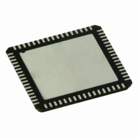
ADC16DV160CILQ/NOPB National Semiconductor, ADC16DV160CILQ/NOPB Datasheet - Page 5

ADC16DV160CILQ/NOPB
Manufacturer Part Number
ADC16DV160CILQ/NOPB
Description
ADC 16BIT DUAL 160MSPS 68LLP
Manufacturer
National Semiconductor
Series
PowerWise®r
Datasheet
1.ADC16DV160CILQNOPB.pdf
(30 pages)
Specifications of ADC16DV160CILQ/NOPB
Number Of Bits
16
Sampling Rate (per Second)
160M
Data Interface
Serial, SPI™
Number Of Converters
2
Power Dissipation (max)
1.47W
Voltage Supply Source
Single Supply
Operating Temperature
-40°C ~ 85°C
Mounting Type
Surface Mount
Package / Case
68-VFQFN, Exposed Pad
Leaded Process Compatible
Yes
Rohs Compliant
Yes
Peak Reflow Compatible (260 C)
Yes
Lead Free Status / RoHS Status
Lead free / RoHS Compliant
Other names
ADC16DV160CILQ
POWER SUPPLIES
0, 3, 15, 18, 21,
4, 14, 22, 64
28 - 43
61 - 46
Pin(s)
44, 45
65, 68
1, 17
62
63
D1/0+/-Q to
D15/14+/-Q
OUTCLK+/-
D1/0+/-I to
D15/14+/-I
DRGND
AGND
Name
V
V
V
A3.0
A1.8
DR
Analog Ground
Analog Power
Analog Power
Analog Power
Ground
Output
Output
Type
Function and Connection
LVDS Data Output. The 16-bit digital output of the data converter is
provided on these ports in a dual data rate manner. A 100Ω termination
resistor must be placed between each pair of differential signals at the
far end of the transmission line. The odd bit data is output first and should
be captured first when de-interleaving the data.
Output Clock. This pin is used to clock the output data. It has the same
frequency as the sampling clock. One word of data is output in each
cycle of this signal. A 100Ω termination resistor must be placed between
the differential clock signals at the far end of the transmission line. The
falling edge of this signal should be used to capture the odd bit data
(D15, D13, D11…D1). The rising edge of this signal should be used to
capture the even bit data (D14, D12, D10…D0).
3.0V Analog Power Supply. These pins should be connected to a quiet
source and should be decoupled to AGND with 0.1 µF capacitors
located close to the power pins.
1.8V Analog Power Supply. These pins should be connected to a quiet
source and should be decoupled to AGND with 0.1 µF capacitors
located close to the power pins.
Analog Ground Return.
Pin 0 is the exposed pad on the bottom of the package. The exposed
pad must be connected to the ground plane to ensure rated
performance.
Output Driver Power Supply. This pin should be connected to a quiet
voltage source and be decoupled to DRGND with a 0.1 µF capacitor
close to the power pins.
Output Driver Ground Return.
5
www.national.com


