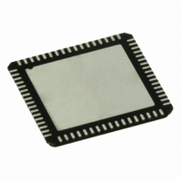
ADC16DV160CILQ/NOPB National Semiconductor, ADC16DV160CILQ/NOPB Datasheet - Page 7

ADC16DV160CILQ/NOPB
Manufacturer Part Number
ADC16DV160CILQ/NOPB
Description
ADC 16BIT DUAL 160MSPS 68LLP
Manufacturer
National Semiconductor
Series
PowerWise®r
Datasheet
1.ADC16DV160CILQNOPB.pdf
(30 pages)
Specifications of ADC16DV160CILQ/NOPB
Number Of Bits
16
Sampling Rate (per Second)
160M
Data Interface
Serial, SPI™
Number Of Converters
2
Power Dissipation (max)
1.47W
Voltage Supply Source
Single Supply
Operating Temperature
-40°C ~ 85°C
Mounting Type
Surface Mount
Package / Case
68-VFQFN, Exposed Pad
Leaded Process Compatible
Yes
Rohs Compliant
Yes
Peak Reflow Compatible (260 C)
Yes
Lead Free Status / RoHS Status
Lead free / RoHS Compliant
Other names
ADC16DV160CILQ
SNR
SFDR
THD
H2
H3
SPUR
POWER SUPPLY CHARACTERISTICS
I
I
I
DIGITAL INPUT CHARACTERISTICS (SCLK, SDIO, CSB)
V
V
I
I
C
DIGITAL OUTPUT CHARACTERISTICS (SDIO)
V
V
A3.0
A1.8
DR
IN1
IN0
IH
IL
OH
OL
IN
Dynamic Converter Electrical Characteristics
Unless otherwise specified, the following specifications apply: V
f
apply for T
Logic and Power Supply Electrical Characteristics
Unless otherwise specified, the following specifications apply: V
f
apply for T
Symbol
Symbol
CLK
CLK
= 160 MSPS at 2.8 V
= 160 MSPS at 2.8 V
A
A
= T
= T
Analog 3.0V Supply Current
Analog 1.8V Supply Current
Output Driver Supply Current
Core Power Consumption
Driver Power Consumption
Total Power Consumption
Power Consumption in Power Down State
Logical “1” Input Voltage
Logical “0” Input Voltage
Logical “1” Input Current
Logical “0” Input Current
Digital Input Capacitance
Logical “1” Output Voltage
Logical “0” Output Voltage
Signal-to-Noise Ratio
Single-tone Spurious Free Dynamic Range
(Note
Total Harmonic Distortion
Second-order Harmonic
Third-order Harmonic
Worst Harmonic or Spurious Tone excluding H2
and H3
Full Power Bandwidth
Crosstalk
MIN
MIN
9)
to T
to T
MAX
MAX
PP
PP
. All other limits apply for T
. All other limits apply for T
, A
, A
IN
IN
Parameter
Parameter
= -1dBFS, LVDS R
= -1dBFS, LVDS R
(Note
(Note
9)
9)
TERM
TERM
A
A
= +25°C, unless otherwise noted.
= +25°C, unless otherwise noted.
= 100Ω, C
= 100Ω, C
Fin = 30 MHz at −1dBFS
Fin = 197 MHz at −1dBFS
Fin = 197 MHz at −7dBFS
Fin = 30 MHz at −1dBFS
Fin = 197 MHz at −1dBFS
Fin = 197 MHz at −7dBFS
Fin = 197 MHz at −1dBFS
Fin = 197 MHz at −7dBFS
Fin = 197 MHz at −1dBFS
Fin = 197 MHz at −7dBFS
Fin = 197 MHz at −1dBFS
Fin = 197 MHz at −7dBFS
Fin = 197 MHz at −1dBFS
Fin = 197 MHz at −7dBFS
-3dB Point
0 MHz tested channel, f
-1dBFS other channel
0 MHz tested channel, f
-1dBFS other channel
Full Operation
Full Operation
Full Operation
V
V
Full Operation
Power down state, no external clock
Sleep state, no external clock
V
V
I
I
OUT
OUT
A3.0
DR
DR
DR
A3.0
A3.0
7
power; Fin = 5MHz Rterm = 100Ω
= 1.9V
= 1.7V
= 0.5 mA, V
= 1.6 mA, V
+ V
= 3.0V, V
= 3.0V, V
L
L
= 5 pF. Typical values are for T
= 5 pF. Typical values are for T
A1.8
power per channel
Conditions
Conditions
(Note
(Note
(Note
(Note
A1.8
A1.8
DR
DR
= 1.8V, V
= 1.8V, V
= 1.8V
= 1.8V
11)
11)
11)
11)
IN
IN
=32.5 MHz at
=192 MHz at
DR
DR
= 1.8V, Differential sinusoidal clock,
= 1.8V, Differential sinusoidal clock,
A
A
Typical Limits
= 25°C. Boldface limits
= 25°C. Boldface limits
−105
1.34
77.3
Typ
−10
−85
−96
−90
−99
−93
102
110
103
345
105
612
117
1.4
4.4
78
76
95
89
99
98
65
60
10
5
Limits
1.47
374
116
74.3
1.2
0.4
1.2
0.4
76
-80
81
90
www.national.com
(Limits)
V (max)
V (max)
V (min)
V (min)
Units
Units
dBFS
dBFS
dBFS
dBFS
dBFS
dBFS
dBFS
dBFS
dBFS
dBFS
dBFS
dBFS
dBFS
dBFS
dBFS
dBFS
mW
mW
mW
mW
GHz
mA
mA
mA
µA
µA
pF
W


