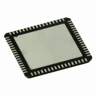
ADC16DV160CILQ/NOPB National Semiconductor, ADC16DV160CILQ/NOPB Datasheet - Page 21

ADC16DV160CILQ/NOPB
Manufacturer Part Number
ADC16DV160CILQ/NOPB
Description
ADC 16BIT DUAL 160MSPS 68LLP
Manufacturer
National Semiconductor
Series
PowerWise®r
Datasheet
1.ADC16DV160CILQNOPB.pdf
(30 pages)
Specifications of ADC16DV160CILQ/NOPB
Number Of Bits
16
Sampling Rate (per Second)
160M
Data Interface
Serial, SPI™
Number Of Converters
2
Power Dissipation (max)
1.47W
Voltage Supply Source
Single Supply
Operating Temperature
-40°C ~ 85°C
Mounting Type
Surface Mount
Package / Case
68-VFQFN, Exposed Pad
Leaded Process Compatible
Yes
Rohs Compliant
Yes
Peak Reflow Compatible (260 C)
Yes
Lead Free Status / RoHS Status
Lead free / RoHS Compliant
Other names
ADC16DV160CILQ
Reference Decoupling
It is highly recommended to place the external decoupling
capacitors connected to V
to the pins as possible. The external decoupling capacitors
should have minimal ESL and ESR. During normal operation,
inappropriate external decoupling with large ESL and/or ESR
capacitors increase the settling time of the ADC core and re-
sult in lower SFDR and SNR performance. The V
be loaded up to 1mA for setting input common mode. The
remaining pins should not be loaded. Smaller capacitor val-
ues might result in degraded noise performance. The decou-
pling capacitor on the V
Additional decoupling on this pin will cause improper calibra-
tion during power-up. All the reference pins except V
a very low output impedance. Driving these pins via a low-
output impedance external circuit for a long time period may
damage the device.
When the V
via transformer, a smaller series resistor should be placed on
the signal path to isolate any switching noise between the
ADC core and input signal. The series resistor introduces a
voltage error between V
while the sampling switches are toggling. The series resis-
tance should not be larger than 50Ω.
All grounds associated with each reference and analog input
pin should be connected to a solid and quiet ground on the
PC board. Coupling noise from digital outputs and their sup-
plies to the reference pins and their ground can cause de-
graded SNR and SFDR performance.
6.0 LAYOUT AND GROUNDING
Proper grounding and proper routing of all signals are essen-
tial to ensure accurate conversion. Maintaining separate ana-
RM
pin is used to set the input common mode level
RM
RP
REF
, V
and V
pin must not exceed 0.1 μF.
RN
, V
CM
RM
FIGURE 13. Internal References and their Decoupling
due to charge injection
and V
REF
pins as close
RM
REF
pin may
have
21
log and digital areas of the board, with the ADC16DV160
between these areas, is required to achieve the specified
performance.
Even though LVDS outputs reduce ground bounce, the pos-
itive and negative signal path have to be well matched, and
their traces should be kept as short as possible. It is recom-
mend to place an LVDS repeater between the ADC16DV160
and digital data receiver block to prevent coupling noise from
the receiving block when the length of the traces are long or
the noise level of the receiving block is high.
Capacitive coupling between the typically noisy digital circuit-
ry and the sensitive analog circuitry can lead to poor perfor-
mance. The solution is to keep the analog circuitry separated
from the digital circuitry, and to keep the clock line as short as
possible.
Since digital switching transients are composed largely of
high frequency components, total ground plane copper
weight will have little effect upon the logic-generated noise.
Because of the skin effect, the total surface area is more im-
portant than its thickness.
Generally, analog and digital lines should not cross. However
whenever it is inevitable, make sure that these lines are
crossing each other at 90° to minimize cross talk. Digital out-
put and output clock signals must be separated from analog
input, references and clock signals unconditionally to ensure
the maximum performance from the ADC16DV160. Any cou-
pling may result in degraded SNR and SFDR performance
especially for high IF applications.
Be especially careful with the layout of inductors and trans-
formers. Mutual inductance can change the characteristics of
the circuit in which they are used. Inductors and transformers
should not be placed side by side, even with just a small part
30101436
www.national.com


