IDT5V49EE702NDGI8 IDT, Integrated Device Technology Inc, IDT5V49EE702NDGI8 Datasheet
IDT5V49EE702NDGI8
Specifications of IDT5V49EE702NDGI8
IDT5V49EE702DLGI8


Related parts for IDT5V49EE702NDGI8


IDT5V49EE702NDGI8 Summary of contents
Page 1
EEPROM PROGRAMMABLE CLOCK GENERATOR Description The IDT5V49EE702 is a programmable clock generator intended for high performance data-communications, telecommunications, consumer, and networking applications. There are four internal PLLs, each individually programmable, allowing for four unique non-integer-related frequencies. The frequencies are generated ...
Page 2
IDT5V49EE702 EEPROM PROGRAMMABLE CLOCK GENERATOR Functional Block Diagram XIN/REF XOUT CLKIN CLKSEL SD/OE SDA Control Logic SCL SEL[2:0] 1. OUT1 & OUT2, OUT3 & OUT6, and OUT5 & OUT5 pairs can be configured to be LVDS, LVPECL or HCSL, or ...
Page 3
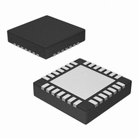
IDT5V49EE702 EEPROM PROGRAMMABLE CLOCK GENERATOR Pin Configuration VDD 1 XOUT 2 XIN/REF 3 VDDx 4 CLKIN 5 GND 6 OUT1 pin VFQFPN (Top View) Pin Descriptions Pin# Pin ...
Page 4
IDT5V49EE702 EEPROM PROGRAMMABLE CLOCK GENERATOR Pin# Pin Name 13 VDDO5 14 GND 15 SDAT 16 SCLK 17 CLKSEL 18 AVDD 19 GND 20 OUT6 21 OUT3 22 VDDO3 23 SEL2 24 SEL1 25 SEL0 26 SD/OE 27 OUT0 28 GND ...
Page 5
IDT5V49EE702 EEPROM PROGRAMMABLE CLOCK GENERATOR PLL Features and Descriptions Pre-Divider 1 (D) Values PLL0 1 - 127 PLL1 1 - 127 PLL2 1 - 127 PLL3 3 - 127 1.For PLL0, PLL1 and PLL2, D=0 means PLL power down. For ...
Page 6
IDT5V49EE702 EEPROM PROGRAMMABLE CLOCK GENERATOR Reference Clock Input Pins and Selection The IDT5V49EE702 supports up to two clock inputs. One of the clock inputs (XIN/ REF) can be driven by either an external crystal or a reference clock. The second ...
Page 7
IDT5V49EE702 EEPROM PROGRAMMABLE CLOCK GENERATOR clocks are at different frequencies, the device will always remain on the primary clock unless it is absent for two secondary clock cycles. The secondary clock must always run at a frequency less than or ...
Page 8
IDT5V49EE702 EEPROM PROGRAMMABLE CLOCK GENERATOR values range from Values of 0 and 7 should not be used. SS_OFFSET[5:0] These bits are used to program the fractional offset with respect to the nominal M integer value. For center ...
Page 9
IDT5V49EE702 EEPROM PROGRAMMABLE CLOCK GENERATOR Profile: Waveform starts with SS_OFFSET, SS_OFFSET + SD SS_OFFSET + SD , etc. J+1 Spread Spectrum Using Sinusoidal Profile Example F = 25MHz 100MHz, Fssc = 33KHz with center IN OUT spread of ...
Page 10
IDT5V49EE702 EEPROM PROGRAMMABLE CLOCK GENERATOR Spread Spectrum Generation (PLL3) PLL3 support spread spectrum generation capability, which users have the option of turning on and off. Spread spectrum profile, frequency, and spread are fully programmable (within limits). The technique is different ...
Page 11
IDT5V49EE702 EEPROM PROGRAMMABLE CLOCK GENERATOR PLL Loop Bandwidth: Charge pump gain (Kφ⎞ 2π VCO gain ( 900 MHz/V * 2π VCO M = Total multiplier value (See the Reference Divider, Feedback Divider and Output Divider ...
Page 12
IDT5V49EE702 EEPROM PROGRAMMABLE CLOCK GENERATOR SEL[2:0] Function The IDT5V49EE702 can support up to six unique configurations. Users may pre-programmed all these configurations, and select the configurations using SEL[2:0] SEL2 SEL1 SEL0 ...
Page 13
IDT5V49EE702 EEPROM PROGRAMMABLE CLOCK GENERATOR Each frame starts with a “Start Condition” and ends with an “End Condition”. These are both generated by the Master device. MSB 7-bit slave address R/W 0 – Slave will ...
Page 14
IDT5V49EE702 EEPROM PROGRAMMABLE CLOCK GENERATOR Progread Note: If the expected read command is not from the next higher register to the previous read or write command, then set a known “read” register address prior to a read operation by issuing ...
Page 15
IDT5V49EE702 EEPROM PROGRAMMABLE CLOCK GENERATOR Bus DC Characteristics Symbol Parameter V Input HIGH Level IH V Input LOW Level IL V Hysteresis of Inputs HYS I Input Leakage Current IN V Output LOW Voltage ...
Page 16
IDT5V49EE702 EEPROM PROGRAMMABLE CLOCK GENERATOR Bus AC Characteristics for Fast Mode Symbol Parameter F Serial Clock Frequency (SCL) SCLK t Bus free time between STOP and START BUF t Setup Time, START SU:START t Hold Time, START ...
Page 17
IDT5V49EE702 EEPROM PROGRAMMABLE CLOCK GENERATOR Absolute Maximum Ratings Stresses above the ratings listed below can cause permanent damage to the IDT5V49EE702. These ratings, which are standard values for IDT commercially rated parts, are stress ratings only. Functional operation of the ...
Page 18
IDT5V49EE702 EEPROM PROGRAMMABLE CLOCK GENERATOR Capacitance (T = +25 °C) A Symbol C Input Capacitance (CLKIN, CLKSEL, SD/OE, IN SDA, SCL, SEL[2:0]) Pull-down CLKIN, CLKSEL, SD/OE, SEL[2:0] Resistor Crystal Specifications XTAL_FREQ Crystal frequency XTAL_MIN Minimum crystal load capacitance XTAL_MAX Maximum ...
Page 19
IDT5V49EE702 EEPROM PROGRAMMABLE CLOCK GENERATOR DC Electrical Characteristics for LVDS Symbol V (+) Differential Output Voltage for the TRUE binary state OT V (-) Differential Output Voltage for the FALSE binary state OT V Change in V between Complimentary Output ...
Page 20
IDT5V49EE702 EEPROM PROGRAMMABLE CLOCK GENERATOR Symbol Parameter I Total Power V Supply TOT DD Current Note 1: Output bank 5 is toggling. Other output banks are powered down. Note 2: The termination resistors are excluded from these measurements. DC Electrical ...
Page 21
IDT5V49EE702 EEPROM PROGRAMMABLE CLOCK GENERATOR AC Timing Electrical Characteristics (Spread Spectrum Generation = OFF) Symbol Parameter 1 f Input Frequency Output Frequency f VCO Frequency VCO f PFD Frequency PFD f Loop Bandwidth BW t2 Input ...
Page 22
IDT5V49EE702 EEPROM PROGRAMMABLE CLOCK GENERATOR Symbol Parameter t7 Clock Jitter t8 Output Skew 4 t9 Lock Time 5 t10 Lock Time 1.Practical lower frequency is determined by loop filter settings. 2.A slew rate of 2.75V/ns or greater should be selected ...
Page 23
IDT5V49EE702 EEPROM PROGRAMMABLE CLOCK GENERATOR Test Circuits and Conditions V DDOx V DD 0.1µF IDT® EEPROM PROGRAMMABLE CLOCK GENERATOR OUTx 0.1µF GND Test Circuits for DC Outputs 23 CLOCK SYNTHESIZER CLK OUT C L IDT5V49EE702 REV F 022310 ...
Page 24
IDT5V49EE702 EEPROM PROGRAMMABLE CLOCK GENERATOR Other Termination Scheme (Block Diagram) OUTx 5 pF GND LVTTL for each output 5 pF OUTx 5 pF GND LVPECL IDT® EEPROM PROGRAMMABLE CLOCK GENERATOR CLK OUT V -2V DD 49.9 Ohm CLK ...
Page 25
IDT5V49EE702 EEPROM PROGRAMMABLE CLOCK GENERATOR Programming Registers Table Default Register Addr Hex 7 6 Value 0x00 00 0x01 00 SP OE6 0x02 02 0x03 02 Reserved 0x04 0F SH 0x05 04 Reserved 0x06 00 0x07 00 Reserved 0x08 00 0x09 ...
Page 26
IDT5V49EE702 EEPROM PROGRAMMABLE CLOCK GENERATOR Default Register Addr Hex 7 6 Value 0x28 00 Reserved 0x29 00 Reserved 0x2A 00 Reserved 0x2B 00 Reserved 0x2C 00 Reserved 0x2D 00 Reserved 0x2E 01 0x2F 01 0x30 01 0x31 01 0x32 01 ...
Page 27
IDT5V49EE702 EEPROM PROGRAMMABLE CLOCK GENERATOR Default Register Addr Hex 7 6 Value 0x56 00 IP3[3:0]_CFG4 0x57 00 IP3[3:0]_CFG5 0x58 00 IP3[3:0]_CFG0 0x59 00 IP3[3:0]_CFG1 0x5A 00 IP3[3:0]_CFG2 0x5B 00 IP3[3:0]_CFG3 0x5C 03 Reserved 0x5D 03 Reserved 0x5E 03 Reserved 0x5F ...
Page 28
IDT5V49EE702 EEPROM PROGRAMMABLE CLOCK GENERATOR Default Register Addr Hex 7 6 Value 0x77 00 0x78 00 OEM3[1:0] 0x79 00 0x7A 00 OEM5[1:0] 0x7B 00 0x7C 00 0x7D 00 0x7E 00 0x7F 00 0x80 00 0x81 00 0x82 00 0x83 00 ...
Page 29
IDT5V49EE702 EEPROM PROGRAMMABLE CLOCK GENERATOR Default Register Addr Hex 7 6 Value 0xA7 7F PM6_CFG5 0xA8 7F PM6_CFG0 0xA9 7F PM6_CFG1 0xAA 7F PM6_CFG2 0xAB 7F PM6_CFG3 0xAC 00 TSSC[3:0]_CFG0 0xAD 00 TSSC[3:0]_CFG1 0xAE 00 TSSC[3:0]_CFG2 0xAF 00 TSSC[3:0]_CFG3 0xB0 ...
Page 30
IDT5V49EE702 EEPROM PROGRAMMABLE CLOCK GENERATOR Default Register Addr Hex 7 6 Value 0xCA 49 SRC6[2:0]_CFG4 0xCB 49 SRC6[2:0]_CFG5 0xCC 49 SRC6[2:0]_CFG0 0xCD 49 SRC6[2:0]_CFG1 0xCE 49 SRC6[2:0]_CFG2 0xCF 49 SRC6[2:0]_CFG3 Default Configuration: OUT1 = Reference Clock output, all other outputs ...
Page 31
IDT5V49EE702 EEPROM PROGRAMMABLE CLOCK GENERATOR Marking Diagram 4702DI #YYWW$ Notes: 1. “#” is the lot number. 2. YYWW is the last two digits of the year and week that the part was assembled. 3. “$” is the assembly mark code. ...
Page 32
IDT5V49EE702 EEPROM PROGRAMMABLE CLOCK GENERATOR Package Outline and Package Dimensions Package dimensions are kept current with JEDEC Publication No. 95 Index Area Top View D Millimeters Symbol Min Max A 0.80 1. 0.05 A3 ...
Page 33
IDT5V49EE702 EEPROM PROGRAMMABLE CLOCK GENERATOR Revision History Rev. Originator Date Description of Change A R.Willner 4/27/09 Advance Information. B R.Willner 5/04/09 Identified VDDX (crystal oscillator power) and AVDD (analog power) on device. C R.Willner 6/04/09 Add default configurations, pull-down resistor ...
Page 34
IDT5V49EE702 EEPROM PROGRAMMABLE CLOCK GENERATOR Innovate with IDT and accelerate your future networks. Contact: www.IDT.com For Sales 800-345-7015 408-284-8200 Fax: 408-284-2775 Corporate Headquarters Integrated Device Technology, Inc. www.idt.com © 2010 Integrated Device Technology, Inc. All rights reserved. Product specifications subject ...