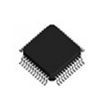
MPC9600AE IDT, Integrated Device Technology Inc, MPC9600AE Datasheet - Page 11

MPC9600AE
Manufacturer Part Number
MPC9600AE
Description
IC PLL CLK DRIVER LV 48-LQFP
Manufacturer
IDT, Integrated Device Technology Inc
Type
PLL Clock Driverr
Datasheet
1.MPC9600AER2.pdf
(14 pages)
Specifications of MPC9600AE
Pll
Yes with Bypass
Input
LVCMOS, LVPECL
Output
LVCMOS
Number Of Circuits
1
Ratio - Input:output
2:22
Differential - Input:output
Yes/No
Frequency - Max
200MHz
Divider/multiplier
Yes/No
Voltage - Supply
2.375 V ~ 3.465 V
Operating Temperature
-40°C ~ 85°C
Mounting Type
Surface Mount
Package / Case
48-LQFP
Frequency-max
200MHz
Number Of Elements
1
Supply Current
5mA
Pll Input Freq (min)
16.67MHz
Pll Input Freq (max)
50MHz
Operating Supply Voltage (typ)
2.5/3.3V
Operating Temp Range
-40C to 85C
Package Type
TQFP
Output Frequency Range
50 to 200MHz
Operating Supply Voltage (min)
2.375V
Operating Supply Voltage (max)
3.465V
Operating Temperature Classification
Industrial
Pin Count
48
Lead Free Status / RoHS Status
Lead free / RoHS Compliant
Available stocks
Company
Part Number
Manufacturer
Quantity
Price
Company:
Part Number:
MPC9600AE
Manufacturer:
IDT, Integrated Device Technology Inc
Quantity:
10 000
Company:
Part Number:
MPC9600AER2
Manufacturer:
IDT
Quantity:
1 186
Company:
Part Number:
MPC9600AER2
Manufacturer:
Sigmatel
Quantity:
77
Company:
Part Number:
MPC9600AER2
Manufacturer:
IDT, Integrated Device Technology Inc
Quantity:
10 000
Part Number:
MPC9600AER2
Manufacturer:
FESSCALE
Quantity:
20 000
reflection coefficient, to 2.6 V. It will then increment towards the
quiescent 3.0 V in steps separated by one round trip delay (in this
case 4.0 ns).
IDT™ / ICS™ 2.5V AND 3.3V LVCMOS PLL CLOCK DRIVER
MPC9600
LOW VOLTAGE, 2.5V AND 3.3V LVCMOS PLL CLOCK DRIVER
At the load end the voltage will double due to the near unity
3.0
2.5
2.0
1.5
1.0
0.5
0
Figure 9. Single versus Dual Waveforms
t
D
2
= 3.8956
OutA
In
4
Differential Pulse
Generator
Generator
Z = 50 Ω
6
Z = 50 Ω
Pulse
Time (ns)
t
D
= 3.9386
OutB
8
10
Figure 11. CCLK MPC9600 AC Test Reference
Figure 12. PCLK MPC9600 AC Test Reference
Z
O
V
= 50 Ω
TT
12
Z
O
R
R
= 50 Ω
T
T
= 50 Ω
= 50 Ω
14
V
TT
MPC9600 DUT
MPC9600 DUT
11
cause any false clock triggering, however designers may be
uncomfortable with unwanted reflections on the line. To better
match the impedances when driving multiple lines the situation in
Figure 10
resistors are reduced such that when the parallel combination is
added to the output buffer impedance the line impedance is
perfectly matched.
the MPC9600 clock driver circuit.
Since this step is well above the threshold region it will not
The following figures illustrate the measurement reference for
Figure 10. Optimized Dual Line Termination
should be used. In this case the series terminating
MPC9600
Output
14 Ω
Buffer
Z
Z
14 Ω + 22 Ω || 22 Ω = 50 Ω || 50 Ω
O
O
= 50 Ω
= 50 Ω
R
R
T
T
= 50 Ω
= 50 Ω
25 Ω = 25 Ω
R
R
S
S
= 22 Ω
= 22 Ω
MPC9600 REV. 5 NOVEMBER 10, 2008
V
V
TT
TT
Z
Z
O
O
= 50 Ω
= 50 Ω


