MPC9600AE IDT, Integrated Device Technology Inc, MPC9600AE Datasheet
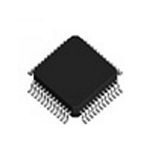
IC PLL CLK DRIVER LV 48-LQFP

MPC9600AE

Manufacturer Part Number
MPC9600AE
Description
IC PLL CLK DRIVER LV 48-LQFP
Manufacturer
IDT, Integrated Device Technology Inc
Type
PLL Clock Driverr
Datasheet

Specifications of MPC9600AE

Pll
Yes with Bypass
Input
LVCMOS, LVPECL
Output
LVCMOS
Number Of Circuits
1
Ratio - Input:output
2:22
Differential - Input:output
Yes/No
Frequency - Max
200MHz
Divider/multiplier
Yes/No
Voltage - Supply
2.375 V ~ 3.465 V
Operating Temperature
-40°C ~ 85°C
Mounting Type
Surface Mount
Package / Case
48-LQFP
Frequency-max
200MHz
Number Of Elements
1
Supply Current
5mA
Pll Input Freq (min)
16.67MHz
Pll Input Freq (max)
50MHz
Operating Supply Voltage (typ)
2.5/3.3V
Operating Temp Range
-40C to 85C
Package Type
TQFP
Output Frequency Range
50 to 200MHz
Operating Supply Voltage (min)
2.375V
Operating Supply Voltage (max)
3.465V
Operating Temperature Classification
Industrial
Pin Count
48
Lead Free Status / RoHS Status
Lead free / RoHS Compliant

Available stocks

Company
Part Number
Manufacturer
Quantity
Price
Part Number:
MPC9600AE
Manufacturer:
IDT, Integrated Device Technology Inc
Quantity:
10 000
Part Number:
MPC9600AER2
Manufacturer:
IDT
Quantity:
1 186
Part Number:
MPC9600AER2
Manufacturer:
Sigmatel
Quantity:
77
Part Number:
MPC9600AER2
Manufacturer:
IDT, Integrated Device Technology Inc
Quantity:
10 000
Part Number:
MPC9600AER2
Manufacturer:
FESSCALE
Quantity:
20 000
LOW VOLTAGE, 2.5V AND 3.3V LVCMOS
PLL CLOCK DRIVER
and fanout buffer. With output frequencies up to 200 MHz and output skews of 150 ps, the
device meets the needs of the most demanding clock tree applications.
Features
Functional Description
MPC9600 has the capability to generate clock signals of 50 to 200 MHz from clock
sources of 16.67 to 50 MHz. The internal PLL is optimized for this frequency range and
does not require external loop filter components. QFB provides an output for the external
feedback path to the feedback input FB_IN. The QFB divider ratio is configurable and
determines the PLL frequency multiplication factor when QFB is directly connected to FB_IN. The MPC9600 is optimized for minimizing
the propagation delay between the clock input and FB_IN.
feedback and output divider ratios, the MPC9600 is capable to multiply the input frequency by 2, 3, 4, and 6.
fanout buffers for the inner branches of the clock distribution tree. All control inputs accept LVCMOS compatible levels. The outputs provide
low impedance LVCMOS outputs capable of driving parallel terminated 50 Ω transmission to V
MPC9600 can drive two lines per output giving the device an effective total fanout of 1:42. With guaranteed maximum output-to-output
skew of 150 ps, the MPC9600 PLL clock driver meets the synchronization requirements of the most demanding systems.
will bypass the PLL.
IDT™ / ICS™ 2.5V AND 3.3V LVCMOS PLL CLOCK DRIVER
The MPC9600 is a low voltage 2.5 V or 3.3 V compatible, 1:21 PLL based clock driver
The MPC9600 is a fully LVCMOS 2.5 V or 3.3 V compatible PLL clock driver. The
Three output banks of 7 outputs each bank can be individually configured to divide the VCO frequency by 2 or by 4. Combining the
The reference clock is selectable either LVPECL or LVCMOS. The LVPECL reference clock feature allows the designer to use LVPECL
The V
The device is packaged in a 48-lead LQFP package to provide optimum combination of board density and performance.
Multiplication of Input Frequency by 2, 3, 4, and 6
Distribution of Output Frequency to 21 Outputs Organized in Three Output Banks:
QA0-QA6, QB0-QB6, QC0-QC6, Each Fully Selectable
Fully Integrated PLL
Selectable Output Frequency Range Is 50 to 100 MHz and 100 to 200 MHz
Selectable Input Frequency Range Is 16.67 to 33 MHz and 25 to 50 MHz
LVCMOS Outputs
Outputs Disable to High Impedance (Except QFB)
LVCMOS or LVPECL Reference Clock Options
48-Lead QFP Packaging
48-Lead Pb-Free Package Available
± 50 ps Cycle-to-Cycle Jitter
150 ps Maximum Output-to-Output Skew
200 ps Maximum Static Phase Offset Window
CCA
analog power pin doubles as a PLL bypass select line for test purpose. When the V
1
TT
CCA
= V
MPC9600 REV. 5 NOVEMBER 10, 2008
CC
is driven to GND the reference clock
48-LEAD LQFP PACKAGE
/2. For series terminated lines the
LOW VOLTAGE CMOS
PLL CLOCK DRIVER
Pb-FREE PACKAGE
3.3 V OR 2.5 V
CASE 932-03
CASE 932-03
FA SUFFIX
AE SUFFIX
SCALE 2:1
SCALE 2:1
MPC9600

Related parts for MPC9600AE

MPC9600AE Summary of contents

Page 1

LOW VOLTAGE, 2.5V AND 3.3V LVCMOS PLL CLOCK DRIVER The MPC9600 is a low voltage 2 3.3 V compatible, 1:21 PLL based clock driver and fanout buffer. With output frequencies up to 200 MHz and output skews of ...

Page 2

MPC9600 LOW VOLTAGE, 2.5V AND 3.3V LVCMOS PLL CLOCK DRIVER (Pulldown) CCLK (Pulldown) PCLK PCLK (Pullup) REF_SEL (Pulldown) FB_IN (Pullup) FSELA (Pullup) FSELB (Pullup) FSELC (Pullup) FSEL_FB (Pulldown) OE IDT™ / ICS™ 2.5V AND 3.3V LVCMOS PLL ...

Page 3

MPC9600 LOW VOLTAGE, 2.5V AND 3.3V LVCMOS PLL CLOCK DRIVER Table 1. Pin Configuration – 48 LQFP Pin I/O PCLK, PCLK Input PECL CCLK Input LVCMOS FB_IN Input LVCMOS QAn Output LVCMOS QBn Output LVCMOS QCn Output LVCMOS QFB Output ...

Page 4

MPC9600 LOW VOLTAGE, 2.5V AND 3.3V LVCMOS PLL CLOCK DRIVER Table 2. Function Table (Controls) Control Pin REF_SEL V CCA OE FSELA FSELB FSELC FSEL_FB GND, PLL off and bypassed for static test and diagnosis. CCA Table ...

Page 5

MPC9600 LOW VOLTAGE, 2.5V AND 3.3V LVCMOS PLL CLOCK DRIVER Table 5. DC Characteristics (V CC Symbol Characteristics V Input High Voltage IH V Input Low Voltage IL V Peak-to-Peak Input Voltage (DC) PP (1) V Common Mode Range (DC) ...

Page 6

MPC9600 LOW VOLTAGE, 2.5V AND 3.3V LVCMOS PLL CLOCK DRIVER Table 7. AC Characteristics – 48 LQFP (V Symbol Characteristics f Input Frequency ref f VCO Frequency VCO f Maximum Output Frequency MAX f Reference Input Duty Cycle refDC V ...

Page 7

MPC9600 LOW VOLTAGE, 2.5V AND 3.3V LVCMOS PLL CLOCK DRIVER Programming the MPC9600 The MPC9600 clock driver outputs can be configured into several divider modes. Additionally the external feedback of the device allows for flexibility in establishing various input to ...

Page 8

MPC9600 LOW VOLTAGE, 2.5V AND 3.3V LVCMOS PLL CLOCK DRIVER Table 9. Typical and Maximum Period Jitter Specification Device Configuration All output banks in ÷ ÷ 4 divider configuration ÷ 2 (FSELA = 0 and FESLB = 0 ...

Page 9

MPC9600 LOW VOLTAGE, 2.5V AND 3.3V LVCMOS PLL CLOCK DRIVER Power Supply Filtering The MPC9600 is a mixed analog/digital product. Its analog circuitry is naturally susceptible to random noise, especially if this noise is seen on the power supply pins. ...

Page 10

MPC9600 LOW VOLTAGE, 2.5V AND 3.3V LVCMOS PLL CLOCK DRIVER Due to the statistical nature of I/O jitter a RMS value (1 σ) is specified. I/O jitter numbers for other confidence factors (CF) can be derived from Table 11. Table ...

Page 11

MPC9600 LOW VOLTAGE, 2.5V AND 3.3V LVCMOS PLL CLOCK DRIVER At the load end the voltage will double due to the near unity reflection coefficient will then increment towards the quiescent 3 steps separated ...

Page 12

MPC9600 LOW VOLTAGE, 2.5V AND 3.3V LVCMOS PLL CLOCK DRIVER PCLK V PP PCLK FB_IN t (∅) Figure 14. Propagation Delay (t , status phase offset) Ø Test Reference 100% P ...

Page 13

MPC9600 LOW VOLTAGE, 2.5V AND 3.3V LVCMOS PLL CLOCK DRIVER 4X 0.200 AB T 0.200 AC T BASE METAL N J ...

Page 14

MPC9600 LOW VOLTAGE, 2.5V AND 3.3V LVCMOS PLL CLOCK DRIVER Contact Information: www.IDT.com Sales 800-345-7015 (inside USA) +408-284-8200 (outside USA) Fax: 408-284-2775 www.IDT.com/go/contactIDT © 2008 Integrated Device Technology, Inc. All rights reserved. Product specifications subject to change without notice. IDT ...

Related keywords