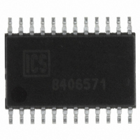
ICS87004AGLF IDT, Integrated Device Technology Inc, ICS87004AGLF Datasheet - Page 10

ICS87004AGLF
Manufacturer Part Number
ICS87004AGLF
Description
IC CLK GENERATOR ZD 1:4 24-TSSOP
Manufacturer
IDT, Integrated Device Technology Inc
Series
HiPerClockS™r
Type
Clock Generator, Fanout Distribution, Multiplexer , Zero Delay Bufferr
Datasheet
1.ICS87004AGLF.pdf
(15 pages)
Specifications of ICS87004AGLF
Pll
Yes with Bypass
Input
HCSL, LVDS, LVHSTL, LVPECL, SSTL
Output
LVCMOS, LVTTL
Number Of Circuits
1
Ratio - Input:output
2:4
Differential - Input:output
Yes/No
Frequency - Max
250MHz
Divider/multiplier
Yes/Yes
Voltage - Supply
2.375 V ~ 3.465 V
Operating Temperature
0°C ~ 70°C
Mounting Type
Surface Mount
Package / Case
24-TSSOP
Frequency-max
250MHz
Lead Free Status / RoHS Status
Lead free / RoHS Compliant
Other names
800-1192
800-1192-5
800-1192
87004AGLF
800-1192-5
800-1192
87004AGLF
Available stocks
Company
Part Number
Manufacturer
Quantity
Price
Company:
Part Number:
ICS87004AGLF
Manufacturer:
IDT Integrated Device Technolo
Quantity:
135
Company:
Part Number:
ICS87004AGLF
Manufacturer:
IDT
Quantity:
91
ICS87004 Data Sheet
Application Information
Power Supply Filtering Technique
As in any high speed analog circuitry, the power supply pins are
vulnerable to random noise. To achieve optimum jitter performance,
power supply isolation is required. The ICS87004 provides separate
power supplies to isolate any high switching noise from the outputs
to the internal PLL. V
connected to the power supply plane through vias, and 0.01µF
bypass capacitors should be used for each pin. Figure 1 illustrates
this for a generic V
additional 10Ω resistor along with a 10µF bypass capacitor be
connected to the V
a ferrite bead.
Wiring the Differential Input to Accept Single Ended Levels
Figure 2 shows how the differential input can be wired to accept
single ended levels. The reference voltage V_REF = V
generated by the bias resistors R1, R2 and C1. This bias circuit
should be located as close as possible to the input pin. The ratio of
R1 and R2 might need to be adjusted to position the V_REF in the
center of the input voltage swing. For example, if the input clock swing
is only 2.5V and V
0.609.
Recommendations for Unused Input and Output Pins
Inputs:
CLK/nCLK Inputs
For applications not requiring the use of the differential input, both
CLK and nCLK can be left floating. Though not required, but for
additional protection, a 1kΩ resistor can be tied from CLK to ground.
LVCMOS Control Pins
All control pins have internal pullups or pulldowns; additional
resistance is not required but can be added for additional protection.
A 1kΩ resistor can be used.
ICS87004AG REVISION C DECEMBER 1, 2009
DD
DDA
DD
DD,
= 3.3V, V_REF should be 1.25V and R2/R1 =
pin and also shows that V
pin. The 10Ω resistor can also be replaced by
V
DDA
and V
DDO
should be individually
DDA
requires that an
DD
/2 is
10
Figure 2. Single-Ended Signal Driving Differential Input
Outputs:
LVCMOS Outputs
All unused LVCMOS output can be left floating. There should be no
trace attached.
1:4, DIFFERENTIAL-TO-LVCMOS/LVTTL ZERO DELAY CLOCK GENERATOR
Single Ended Clock Input
Figure 1. Power Supply Filtering
C1
0.1u
V_REF
V
V
DDA
DD
©2009 Integrated Device Technology, Inc.
.01µF
.01µF
3.3V or 2.5V
R1
1K
R2
1K
V
DD
10Ω
10µF
CLKx
nCLKx


