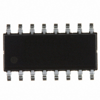
ICS307M-02ILFT IDT, Integrated Device Technology Inc, ICS307M-02ILFT Datasheet - Page 6

ICS307M-02ILFT
Manufacturer Part Number
ICS307M-02ILFT
Description
IC CLOCK SOURCE PROGR 16-SOIC
Manufacturer
IDT, Integrated Device Technology Inc
Type
Clock Generatorr
Datasheet
1.ICS307M-02LFT.pdf
(10 pages)
Specifications of ICS307M-02ILFT
Pll
Yes with Bypass
Input
Clock, Crystal
Output
LVCMOS
Number Of Circuits
1
Ratio - Input:output
2:2
Differential - Input:output
No/No
Frequency - Max
180MHz
Divider/multiplier
Yes/No
Voltage - Supply
3 V ~ 5.5 V
Operating Temperature
-40°C ~ 85°C
Mounting Type
Surface Mount
Package / Case
16-SOIC
Frequency-max
180MHz
Number Of Elements
1
Pll Input Freq (min)
2MHz
Pll Input Freq (max)
50MHz
Operating Supply Voltage (typ)
3.3/5V
Operating Temp Range
-40C to 85C
Package Type
SOIC N
Output Frequency Range
6 to 180MHz
Operating Supply Voltage (min)
3V
Operating Supply Voltage (max)
5.5V
Operating Temperature Classification
Industrial
Pin Count
16
Lead Free Status / RoHS Status
Lead free / RoHS Compliant
Other names
307M-02ILFT
800-1797-2
800-1797-2
Available stocks
Company
Part Number
Manufacturer
Quantity
Price
Company:
Part Number:
ICS307M-02ILFT
Manufacturer:
ADI
Quantity:
211
IDT™ / ICS™ SERIALLY PROGRAMMABLE CLOCK SOURCE
ICS307-01/-02
SERIALLY PROGRAMMABLE CLOCK SOURCE
Programming Example
AC Parameters for Writing to the ICS307
External Components/Crystal Selection
The ICS307 requires a 0.01 F decoupling capacitor to be connected between VDD and GND. It must be connected
close to the ICS307 to minimize lead inductance. A 33 terminating resistor can be used in series with CLK1 and
CLK2 outputs. A parallel resonant, fundamental mode crystal with a load (correlation) capacitance of C should be
used, where C is the value calculated from Table 4. For crystals with a specified load capacitance greater than C,
additional crystal capacitors may be connected from each of the pins X1 and X2 to ground as shown in the Block
Diagram on page 1. The value (in pF) of these crystal caps should be = (C
capacitance in pF and C is the capacitance value from Table 4. These external capacitors are only required for
applications where the exact frequency is critical. For a clock input, connect to X1 and leave X2 unconnected (no
capacitors on either pin).
To generate 66.66 MHz from a 14.31818 MHz input, the RDW should be 59, the VDW should be 276, and
the Output Divide is 2. Selecting the minimum internal load capacitance, CMOS duty cycle, and CLK2 to be
OFF means that the following three bytes are sent to the ICS307:
As show in Figure 2, after these 24 bits are clocked into the ICS307, taking STROBE high will send this
data to the internal latch and the CLK output will lock within 10 ms.
Note: If STROBE is in the high state and SCLK is pulsed, DATA is clocked directly to the internal latch and
the output conditions will change accordingly. Although this will not damage the ICS307, it is recommended
that STROBE be kept low while DATA is being clocked into the ICS307 in order to avoid unintended
changes on the output clocks.
t
DATA
STROBE
SCLK
setup
Figure 2. Timing Diagram for Programming the ICS307
Parameter
t
t
SETUP
C1
HOLD
t
t
W
S
00110001
Byte 1
C0
TTL
t
hold
F1
Hold time after SCLK
Strobe pulse width
SCLK Frequency
Data wait time
Setup time
Condition
R1
10001010
6
Byte 2
R0
t
w
t
s
Min.
L
10
10
10
40
-C)*2, where C
SER PROG CLOCK SYNTHESIZER
Max.
50
L
00111011
is the crystal load
Byte 3
ICS307-01/-02 REV J 051310
Units
MHz
ns
ns
ns
ns


