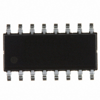
ICS307M-02ILFT IDT, Integrated Device Technology Inc, ICS307M-02ILFT Datasheet

ICS307M-02ILFT
Specifications of ICS307M-02ILFT
800-1797-2
Available stocks
Related parts for ICS307M-02ILFT
ICS307M-02ILFT Summary of contents
Page 1
SERIALLY PROGRAMMABLE CLOCK SOURCE Description The ICS307-01 and ICS307-02 are versatile serially programmable clock sources which take up very little board space. They can generate any frequency from 6 to 200 MHz and have a second configurable output. The outputs ...
Page 2
ICS307-01/-02 SERIALLY PROGRAMMABLE CLOCK SOURCE Pin Assignment X1/ICLK VDD CLK2 SCLK 8 16 pin (150 m il Pin Descriptions Pin Pin Number Name 1 X1/ICLK 2 ...
Page 3
ICS307-01/-02 SERIALLY PROGRAMMABLE CLOCK SOURCE Determining the Output Frequency On power-up, the ICS307-01 on-chip registers can have random values so almost any frequency may be output from the part. CLK1 will always have some clock signal present, but CLK2 could ...
Page 4
ICS307-01/-02 SERIALLY PROGRAMMABLE CLOCK SOURCE Setting the Device Characteristics The tables below show the settings which can be configured, as well as the VCO and Reference dividers. Table 1. Output Divide and Maximum Output Frequency CLK1 Output ...
Page 5
ICS307-01/-02 SERIALLY PROGRAMMABLE CLOCK SOURCE Bypass Mode If R6:0 is programmed to 0000000, the PLL is powered down and bypassed; the reference frequency will come from both CLK1 and CLK2 possible to generate glitches going into and out ...
Page 6
ICS307-01/-02 SERIALLY PROGRAMMABLE CLOCK SOURCE Programming Example To generate 66.66 MHz from a 14.31818 MHz input, the RDW should be 59, the VDW should be 276, and the Output Divide is 2. Selecting the minimum internal load capacitance, CMOS duty ...
Page 7
ICS307-01/-02 SERIALLY PROGRAMMABLE CLOCK SOURCE Absolute Maximum Ratings Stresses above the ratings listed below can cause permanent damage to the ICS307-01/-02. These ratings, which are standard values for IDT commercially rated parts, are stress ratings only. Functional operation of the ...
Page 8
ICS307-01/-02 SERIALLY PROGRAMMABLE CLOCK SOURCE Parameter Short Circuit Current Input Capacitance On-Chip Pull-up Resistor AC Electrical Characteristics VDD = 3.3 V ±5%, Ambient Temperature 0 to +70 C, unless stated otherwise Parameter Input Frequency Output Frequency (see Table 1) Output ...
Page 9
... ICS307M-02LF 307M-02LFT ICS307M-02LF 307M-02ILF 307M-02ILF 307M-02ILFT 307M-02ILF "LF" suffix to the part number denotes Pb-Free configuration, RoHS compliant. While the information presented herein has been checked for both accuracy and reliability, Integrated Device Technology (IDT) assumes no responsibility for either its use or for the infringement of any patents or other rights of third parties, which would result from its use. No other circuits, patents, or licenses are implied ...
Page 10
ICS307-01/-02 SERIALLY PROGRAMMABLE CLOCK SOURCE Innovate with IDT and accelerate your future networks. Contact: www.IDT.com For Sales 800-345-7015 408-284-8200 Fax: 408-284-2775 Corporate Headquarters Integrated Device Technology, Inc. www.idt.com www.idt.com/go/clockhelp © 2006 Integrated Device Technology, Inc. All rights reserved. Product specifications ...


