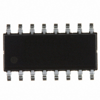
ICS307M-02ILFT IDT, Integrated Device Technology Inc, ICS307M-02ILFT Datasheet - Page 5

ICS307M-02ILFT
Manufacturer Part Number
ICS307M-02ILFT
Description
IC CLOCK SOURCE PROGR 16-SOIC
Manufacturer
IDT, Integrated Device Technology Inc
Type
Clock Generatorr
Datasheet
1.ICS307M-02LFT.pdf
(10 pages)
Specifications of ICS307M-02ILFT
Pll
Yes with Bypass
Input
Clock, Crystal
Output
LVCMOS
Number Of Circuits
1
Ratio - Input:output
2:2
Differential - Input:output
No/No
Frequency - Max
180MHz
Divider/multiplier
Yes/No
Voltage - Supply
3 V ~ 5.5 V
Operating Temperature
-40°C ~ 85°C
Mounting Type
Surface Mount
Package / Case
16-SOIC
Frequency-max
180MHz
Number Of Elements
1
Pll Input Freq (min)
2MHz
Pll Input Freq (max)
50MHz
Operating Supply Voltage (typ)
3.3/5V
Operating Temp Range
-40C to 85C
Package Type
SOIC N
Output Frequency Range
6 to 180MHz
Operating Supply Voltage (min)
3V
Operating Supply Voltage (max)
5.5V
Operating Temperature Classification
Industrial
Pin Count
16
Lead Free Status / RoHS Status
Lead free / RoHS Compliant
Other names
307M-02ILFT
800-1797-2
800-1797-2
Available stocks
Company
Part Number
Manufacturer
Quantity
Price
Company:
Part Number:
ICS307M-02ILFT
Manufacturer:
ADI
Quantity:
211
IDT™ / ICS™ SERIALLY PROGRAMMABLE CLOCK SOURCE
ICS307-01/-02
SERIALLY PROGRAMMABLE CLOCK SOURCE
Bypass Mode
Configuring the ICS307
The ICS307 can be reprogrammed at any time during operation. If R6:0, V8:0, TTL, or C1:0 are changed, the
frequency will transition smoothly to the new value over about 1 ms, without glitches or short cycles. If S2:0 is
changed, it is possible to generate glitches on CLK1 and also on CLK2 for F1:0 = 1 1.
Changing F1:0 will generate glitches on CLK2.
Power up default values for ICS307-02
The input frequency will come from both outputs.
A warning about using the default configuration with input frequencies lower than 13.75 MHz
Power-down Mode
MSB
C1
0
0
C0
If R6:0 is programmed to 0000000, the PLL is powered down and bypassed; the reference frequency will
come from both CLK1 and CLK2. It is possible to generate glitches going into and out of this mode.
The ICS307 can be programmed to set the output functions and frequencies. The three data bytes are
written in DATA pin in this order:
C1 is loaded into the port first and R0 last.
R6:R0 Reference Divder Word (RDW)
V8:V0
S2:S0
F1:F0
TTL
C1:C0 Internal Load Capacitance for Crystal
The VCO will run only as low as its minimum frequency, which is guaranteed to be no more than 55 MHz.
So, in the powerup default condition, the PLL is guaranteed to lock to the input frequency down to 55/4 =
13.75 MHz. However, the part will typically run much slower. The typical minimum VCO frequency is about
30 - 40 MHz, depending on voltage, temperature, and lot variation; so in the powerup default setting, the
CLK2 output will be a minimum of 7.5 - 10 MHz even if the input frequency is lower than that. The output is
not locked to the reference input and so the frequency is not very stable and the phase noise is higher. In
this condition, the CLK2 output will accurately provide the reference frequency down to 0 Hz because this
signal path bypasses the PLL.
When the PDTS pin is pulled low, the chip will enter the power-down mode, where the output clocks are
tri-stated and the rest of the chip is powered down. The chip can be programmed during power-down
mode, however, if the chip is programmed during operation and enters power-down mode, the registers will
return to their settings and not reset when exiting power-down mode (PDTS pin is pulled high).
1
TTL
0
VCO Divider Word (VDW)
Output Divider Select (OD)
Function of CLK2 Output
Duty Cycle Settings
F1
0
F0
0
S2
1
S1
1
LSB
S0
MSB
0
V8
0
V7
0
V6
0
V5
5
0
V4
1
V3
0
V2
0
LSB
V1
MSB
0
V0
SER PROG CLOCK SYNTHESIZER
0
R6
0
R5
ICS307-01/-02 REV J 051310
0
R4
0
R3
1
R2
1
R1
0
LSB
R0


