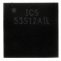
ICS853S12AKILF IDT, Integrated Device Technology Inc, ICS853S12AKILF Datasheet - Page 10

ICS853S12AKILF
Manufacturer Part Number
ICS853S12AKILF
Description
IC FANOUT BUFFER LVPECL 32-VFQFN
Manufacturer
IDT, Integrated Device Technology Inc
Series
HiPerClockS™r
Type
Fanout Buffer (Distribution)r
Datasheet
1.ICS853S12AKILF.pdf
(17 pages)
Specifications of ICS853S12AKILF
Number Of Circuits
1
Ratio - Input:output
1:12
Differential - Input:output
Yes/Yes
Input
CML, LVPECL, SSTL
Output
LVPECL
Frequency - Max
1.5GHz
Voltage - Supply
2.375 V ~ 3.465 V
Operating Temperature
-40°C ~ 85°C
Mounting Type
Surface Mount
Package / Case
32-VFQFN
Frequency-max
1.5GHz
Lead Free Status / RoHS Status
Lead free / RoHS Compliant
Other names
800-1177
853S12AKILF
853S12AKILF
Available stocks
Company
Part Number
Manufacturer
Quantity
Price
Company:
Part Number:
ICS853S12AKILF
Manufacturer:
IDT, Integrated Device Technology Inc
Quantity:
10 000
Company:
Part Number:
ICS853S12AKILFT
Manufacturer:
IDT, Integrated Device Technology Inc
Quantity:
10 000
Part Number:
ICS853S12AKILFT
Manufacturer:
IDT
Quantity:
20 000
The clock layout topology shown below is a typical termination
for LVPECL outputs. The two different layouts mentioned are rec-
ommended only as guidelines.
FOUT and nFOUT are low impedance follower outputs that
generate ECL/LVPECL compatible outputs. Therefore, terminat-
ing resistors (DC current path to ground) or current sources must
be used for functionality. These outputs are designed to drive
IDT
T
ERMINATION FOR
ICS853S12I
LOW SKEW, 1-TO-12, DIFFERENTIAL-TO-3.3V, 2.5V LVPECL FANOUT BUFFER
RTT =
™
/ ICS
™
((V
F
LVPECL FANOUT BUFFER
FOUT
OH
IGURE
+ V
OL
4A. LVPECL O
) / (V
1
3.3V LVPECL O
CC
Z
Z
– 2)) – 2
o
o
= 50Ω
= 50Ω
Z
o
50Ω
UTPUT
T
RTT
ERMINATION
UTPUTS
50Ω
V
CC
FIN
- 2V
10
50Ω transmission lines. Matched impedance techniques should
be used to maximize operating frequency and minimize signal
distortion. Figures 4A and 4B show two different layouts which
are recommended only as guidelines. Other suitable clock lay-
outs may exist and it would be recommended that the board
designers simulate to guarantee compatibility across all printed
circuit and clock component process variations.
FOUT
F
IGURE
4B. LVPECL O
Z
Z
o
o
= 50Ω
= 50Ω
ICS853S12AKI REV. A MAY 21, 2008
125Ω
84Ω
UTPUT
3.3V
125Ω
84Ω
T
ERMINATION
FIN


