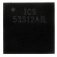
ICS853S12AKILF IDT, Integrated Device Technology Inc, ICS853S12AKILF Datasheet

ICS853S12AKILF
Specifications of ICS853S12AKILF
853S12AKILF
Available stocks
Related parts for ICS853S12AKILF
ICS853S12AKILF Summary of contents
Page 1
LOW SKEW, 1-TO-12, DIFFERENTIAL-TO- 3.3V, 2.5V LVPECL FANOUT BUFFER G D ENERAL ESCRIPTION The ICS853S12I is a low skew, 1-to-12 Differential to-3.3V, 2.5V LVPECL Fanout Buffer and a member HiPerClockS™ of the HiPerClockS™ family of High Performance Clock ...
Page 2
ICS853S12I LOW SKEW, 1-TO-12, DIFFERENTIAL-TO-3.3V, 2.5V LVPECL FANOUT BUFFER ABLE IN ESCRIPTIONS ...
Page 3
ICS853S12I LOW SKEW, 1-TO-12, DIFFERENTIAL-TO-3.3V, 2.5V LVPECL FANOUT BUFFER BSOLUTE AXIMUM ATINGS Supply Voltage, V 4.6V CC Inputs, V -0. Outputs Continuous Current 50mA Surge Current 100mA Package Thermal Impedance, θ JA ...
Page 4
ICS853S12I LOW SKEW, 1-TO-12, DIFFERENTIAL-TO-3.3V, 2.5V LVPECL FANOUT BUFFER 3.3V±5% ABLE HARACTERISTICS ...
Page 5
ICS853S12I LOW SKEW, 1-TO-12, DIFFERENTIAL-TO-3.3V, 2.5V LVPECL FANOUT BUFFER The spectral purity in a band at a specific offset from the fundamental compared to the power of the fundamental is called the dBc Phase Noise. This value is normally expressed ...
Page 6
ICS853S12I LOW SKEW, 1-TO-12, DIFFERENTIAL-TO-3.3V, 2.5V LVPECL FANOUT BUFFER P ARAMETER LVPECL V EE -1.3V ± 0.165V UTPUT OAD EST IRCUIT V CC nPCLK V Cross Points PP PCLK V EE ...
Page 7
ICS853S12I LOW SKEW, 1-TO-12, DIFFERENTIAL-TO-3.3V, 2.5V LVPECL FANOUT BUFFER IRING THE IFFERENTIAL NPUT TO Figure 1 shows how the differential input can be wired to accept single ended levels. The reference voltage V_REF = V generated by ...
Page 8
ICS853S12I LOW SKEW, 1-TO-12, DIFFERENTIAL-TO-3.3V, 2.5V LVPECL FANOUT BUFFER LVPECL LOCK NPUT NTERFACE The PCLK /nPCLK accepts LVPECL, CML, SSTL and other differential signals. Both V and V SWING input requirements. Figures show interface ...
Page 9
ICS853S12I LOW SKEW, 1-TO-12, DIFFERENTIAL-TO-3.3V, 2.5V LVPECL FANOUT BUFFER VFQFN EPAD T R HERMAL ELEASE In order to maximize both the removal of heat from the package and the electrical performance, a land patter n must be incorporated on the ...
Page 10
ICS853S12I LOW SKEW, 1-TO-12, DIFFERENTIAL-TO-3.3V, 2.5V LVPECL FANOUT BUFFER T 3.3V LVPECL O ERMINATION FOR The clock layout topology shown below is a typical termination for LVPECL outputs. The two different layouts mentioned are rec- ommended only as guidelines. FOUT ...
Page 11
ICS853S12I LOW SKEW, 1-TO-12, DIFFERENTIAL-TO-3.3V, 2.5V LVPECL FANOUT BUFFER T 2.5V LVPECL O ERMINATION FOR Figure 5A and Figure 5B show examples of termination for 2.5V LVPECL driver. These terminations are equivalent to terminating 50Ω 2V. For ...
Page 12
ICS853S12I LOW SKEW, 1-TO-12, DIFFERENTIAL-TO-3.3V, 2.5V LVPECL FANOUT BUFFER This section provides information on power dissipation and junction temperature for the ICS853S12I. Equations and example calculations are also provided. 1. Power Dissipation. The total power dissipation for the ICS853S12I is ...
Page 13
ICS853S12I LOW SKEW, 1-TO-12, DIFFERENTIAL-TO-3.3V, 2.5V LVPECL FANOUT BUFFER 3. Calculations and Equations. The purpose of this section is to derive the power dissipated into the load. LVPECL output driver circuit and termination are shown in Figure 6. F IGURE ...
Page 14
ICS853S12I LOW SKEW, 1-TO-12, DIFFERENTIAL-TO-3.3V, 2.5V LVPECL FANOUT BUFFER θ ABLE VS IR LOW ABLE FOR JA Multi-Layer PCB, JEDEC Standard Test Boards T C RANSISTOR OUNT The transistor count for ICS853S12I is: 475 ...
Page 15
ICS853S12I LOW SKEW, 1-TO-12, DIFFERENTIAL-TO-3.3V, 2.5V LVPECL FANOUT BUFFER ACKAGE UTLINE UFFIX FOR NOTE: The following package mechanical drawing is a generic drawing that applies to any pin count VFQFN package. This draw- ...
Page 16
ICS853S12I LOW SKEW, 1-TO-12, DIFFERENTIAL-TO-3.3V, 2.5V LVPECL FANOUT BUFFER ABLE RDERING NFORMATION ...
Page 17
ICS853S12I LOW SKEW, 1-TO-12, DIFFERENTIAL-TO-3.3V, 2.5V LVPECL FANOUT BUFFER Innovate with IDT and accelerate your future networks. Contact: www.IDT.com For Sales 800-345-7015 (inside USA) +408-284-8200 (outside USA) Fax: 408-284-2775 www.IDT.com/go/contactIDT © 2008 Integrated Device Technology, Inc. All rights reserved. Product ...


