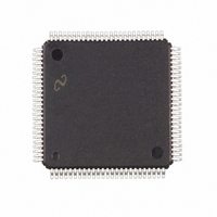
FPD85310VJD National Semiconductor, FPD85310VJD Datasheet - Page 20

FPD85310VJD
Manufacturer Part Number
FPD85310VJD
Description
IC CTRLR PANEL TIMING 100-TQFP
Manufacturer
National Semiconductor
Type
Panel Timing Controllerr
Datasheet
1.FPD85310VJD.pdf
(29 pages)
Specifications of FPD85310VJD
Voltage - Supply
3 V ~ 3.6 V
Operating Temperature
0°C ~ 70°C
Mounting Type
Surface Mount
Package / Case
100-TQFP, 100-VQFP
Lead Free Status / RoHS Status
Contains lead / RoHS non-compliant
Frequency-max
-
Output
-
Input
-
Other names
*FPD85310VJD
Available stocks
Company
Part Number
Manufacturer
Quantity
Price
Company:
Part Number:
FPD85310VJD
Manufacturer:
Texas Instruments
Quantity:
10 000
www.national.com
Functional Description
Note 21: RSTZ transition Low-to-High occurs at the completion of the RPLLS delay or later as shown above.
Note 22: All outputs* forced low in default timing of FPD85310 during power-up delay time.
Note 23: All outputs
Note 24: All outputs
NS recommend to use the continuous download mode.
Note 25: EEPROM download occurs at first detected vertical blanking period.
Note 26: Active outputs depends on INPUT FORMAT register bits [5:6].
Note 27: When configured in ENAB Only Mode (EOM), VSYNC signals are unused except for timing EEPROM DownLoad Sequences. When configured with de-
fault values in Fixed Vertical mode, the VSYNC signal is generated any time ENAB remains low for more than 2 horizontal periods.
During Power Up, before Reset has propagated, the EEPROM may receive spurious addressing that initiates a down load sequence, but the output data is often
not captured for lack of timing alignment with VSYNC. In the case where EEPROM data is not captured during the initial (automatic) Reset or Power Up DownLoad
sequence, Timing Controller outputs are indeterminate until the EEPROM data is successfully loaded, which always begins and is executed at the next VSYNC valid
(low) cycle.
Note 28: During Power Up sequences, false RSTZ signals are possible due to instability of the power supply level, typically within the 10 ms of operation. To avoid
this situation, implementation of the circuit in Figure 17 , or other functional equivalent, is recommended, ( Figure 17 ).
***
**
forced low in continuous download (every two frame) mode.
generate the signal for default values in FPD85310 and unknown values when use the EEPROM values during power-up delay time. Then
FIGURE 16. Power-up Sequence (INPUT FORMAT[6:5] = “01”)
(Continued)
FORMAT
INPUT
[5:6]
00
01
10
11
20
VSYNC# at which
outputs go active
Second VSYNC
Fourth VSYNC
Third VSYNC
Fifth VSYNC
DS101086-10


