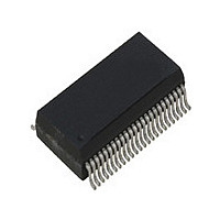
ICS9DB803DFLF IDT, Integrated Device Technology Inc, ICS9DB803DFLF Datasheet - Page 8

ICS9DB803DFLF
Manufacturer Part Number
ICS9DB803DFLF
Description
IC BUFFER 8OUTPUT DIFF 48-SSOP
Manufacturer
IDT, Integrated Device Technology Inc
Type
Clock Bufferr
Series
-r
Datasheet
1.ICS9DB803DFLFT.pdf
(21 pages)
Specifications of ICS9DB803DFLF
Input
HCSL
Output
HCSL, LVDS
Frequency - Max
400MHz
Voltage - Supply
3.135 V ~ 3.465 V
Operating Temperature
0°C ~ 70°C
Mounting Type
Surface Mount
Package / Case
48-SSOP
Frequency-max
400MHz
Number Of Elements
1
Supply Current
200mA
Pll Input Freq (min)
50MHz
Pll Input Freq (max)
110MHz
Operating Supply Voltage (typ)
3.3V
Operating Temp Range
0C to 70C
Package Type
SSOP
Operating Supply Voltage (min)
3.135V
Operating Supply Voltage (max)
3.465V
Operating Temperature Classification
Commercial
Pin Count
48
Lead Free Status / RoHS Status
Lead free / RoHS Compliant
Lead Free Status / RoHS Status
Compliant, Lead free / RoHS Compliant
Other names
9DB803DFLF
Available stocks
Company
Part Number
Manufacturer
Quantity
Price
Company:
Part Number:
ICS9DB803DFLF
Manufacturer:
IDT
Quantity:
40
Company:
Part Number:
ICS9DB803DFLFT
Manufacturer:
IDT
Quantity:
191
IDT
1
2
3
4
5
Electrical Characteristics - Input/Supply/Common Output Parameters
T
Low-level Output Voltage
Guaranteed by design and characterization, not 100% tested in production.
See timing diagrams for timing requirements.
Time from deassertion until outputs are >200 mV
SRC_IN input
The differential input clock must be running for the SMBus to be active
9DB803 Supply Current
9DB403 Supply Current
A
ICS9DB803D
Eight Output Differential Buffer for PCIe for Gen 2
Current sinking at V
Clock/Data Rise Time
Tdrive_SRC_STOP#
Clock/Data Fall Time
9DB803 Powerdown
9DB403 Powerdown
= Tambient for the desired operating range, Supply Voltage V
Input SS Modulation
TM
Input High Voltage
Input High Current
PLL Jitter Peaking
Input Low Voltage
Input Low Current
SMBus Operating
Input Frequency
/ICS
Clk Stabilization
Pin Inductance
PLL Bandwidth
SMBus Voltage
PARAMETER
SCLK/SDATA
SCLK/SDATA
OE# Latency
Capacitance
Tdrive_PD#
Frequency
Frequency
TM
Current
Current
Trise
Tfall
Eight Output Differential Buffer for PCIe Gen 2
OL
SYMBOL
C
I
I
I
I
I
I
F
I
I
f
DD3.3OPC
DD3.3PDC
DD3.3OPC
DD3.3PDC
t
DD3.3OPI
DD3.3OPI
t
I
DD3.3PDI
DD3.3PDI
t
MAXSMB
f
DRVSTP
INSRC_IN
t
T
LATOE#
PULLUP
V
iBYPASS
t
V
C
DRVPD
V
t
F
MODIN
I
JPEAK
BW
RSMB
L
V
FSMB
C
IHSE
I
I
STAB
IHSE
ILSE
iPLL
t
MAX
IL1
IL2
OUT
t
pin
R
OL
F
IN
Full Active, C
Full Active, C
From V
stabilization or de-assertion of PD# to 1st
V
Full Active, C
Full Active, C
Maximum SMBus operating frequency
IN
V
all differential pairs tri-stated, C-Temp
all differential pairs tri-stated, C-Temp
all differential pairs tri-stated, I-Temp
all differential pairs tri-stated, I-temp
Rise time of PD# and SRC_STOP#
IN
Fall time of PD# and SRC_STOP#
= 0 V; Inputs with no pull-up resistors
Single Ended Inputs, 3.3 V +/-5%
Bypass Mode ((Bypass#/PLL= 0)
SRC_IN differential clock inputs
DIF stop after OE# deassertion
= 0 V; Inputs with pull-up resistors
PCIe Mode (Bypass#/PLL= 1)
Logic Inputs, except SRC_IN
DIF start after OE# assertion
-3dB point in High BW Mode
-3dB point in Low BW Mode
all diff pairs driven, C-Temp
all diff pairs driven, C-Temp
all diff pairs driven, I-Temp
DD
all diff pairs driven, I-temp
SRC_Stop# de-assertion
(Triangular Modulation)
Output pin capacitance
DIF output enable after
DIF output enable after
Maximum input voltage
Peak Pass band Gain
Power-Up and after input clock
Allowable Frequency
(Max VIL - 0.15) to
(Min VIH + 0.15) to
PD# de-assertion
(Min VIH + 0.15)
(Max VIL - 0.15)
L
L
CONDITIONS
Temp Range
Temp Range
= Full load; Industrial Temp
= Full load; Industrial Temp
L
L
@ I
V
= Full load; Commerical
= Full load; Commerical
Range
Range
IN
clock
PULLUP
= V
DD
DD
= 3.3 V +/-5%
8
GND - 0.3
-200
MIN
1.5
1.5
0.7
50
33
30
-5
-5
2
2
1
4
100.00
TYP
175
190
105
115
1.5
50
55
25
30
4
6
2
3
3
1
V
DD
1000
MAX
200
225
125
150
110
400
300
300
100
0.8
2.7
1.4
5.5
0.4
60
65
30
35
33
10
5
6
8
3
4
7
5
6
4
2
1
3
5
5
+ 0.3
ICS9DB803D
UNITS NOTES
cycles
MHz
MHz
MHz
MHz
kHz
kHz
mA
mA
mA
mA
mA
mA
mA
mA
mA
mA
mA
mA
mA
nH
ms
uA
uA
uA
pF
pF
pF
dB
ns
us
ns
ns
ns
ns
V
V
V
V
1,4
1,2
1,3
1,3
1,3
1,5
1
1
1
1
1
1
1
1
1
1
1
1
1
1
1
1
1
1
1
1
1
1
1
1
1
1
1
2
1
1
1
1
1
REV J 01/27/11


