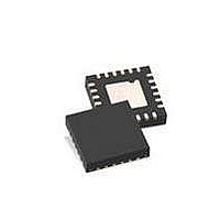
ISP1506BBS,557 NXP Semiconductors, ISP1506BBS,557 Datasheet - Page 22

ISP1506BBS,557
Manufacturer Part Number
ISP1506BBS,557
Description
RF Transceiver USB2.0 ULPI DDR OTG
Manufacturer
NXP Semiconductors
Datasheet
1.ISP1506BBS557.pdf
(80 pages)
Specifications of ISP1506BBS,557
Operating Supply Voltage
1.65 V to 3.6 V
Mounting Style
SMD/SMT
Package / Case
HVQFN-24
Lead Free Status / RoHS Status
Lead free / RoHS Compliant
Other names
935278349557 ISP1506BBS
- Current page: 22 of 80
- Download datasheet (429Kb)
NXP Semiconductors
ISP1506A_ISP1506B_2
Product data sheet
completed. After every reset, an RXCMD is sent to the link to update USB status
information. After this sequence, the ULPI bus is ready for use and the link can start USB
operations.
When the internal PLL is stable, the ISP1506 will drive a 60 MHz clock out from the
CLOCK pin when DIR deasserts. An example start-up sequence is shown in
The recommended power-up sequence for the link is as follows:
The ULPI interface is ready for use.
1. The link waits for 1 ms, ignoring all the ULPI pin status.
2. The link may start to detect DIR status level. If DIR is detected as LOW for three clock
cycles, the link may send a RESET command.
Rev. 02 — 28 August 2008
ISP1506A; ISP1506B
ULPI HS USB OTG transceiver
© NXP B.V. 2008. All rights reserved.
Figure
21 of 79
6.
Related parts for ISP1506BBS,557
Image
Part Number
Description
Manufacturer
Datasheet
Request
R

Part Number:
Description:
ULPI Hi-Speed Universal Serial Bus On-The-Go transceiver
Manufacturer:
NXP [NXP Semiconductors]
Datasheet:
Part Number:
Description:
NXP Semiconductors designed the LPC2420/2460 microcontroller around a 16-bit/32-bitARM7TDMI-S CPU core with real-time debug interfaces that include both JTAG andembedded trace
Manufacturer:
NXP Semiconductors
Datasheet:

Part Number:
Description:
NXP Semiconductors designed the LPC2458 microcontroller around a 16-bit/32-bitARM7TDMI-S CPU core with real-time debug interfaces that include both JTAG andembedded trace
Manufacturer:
NXP Semiconductors
Datasheet:
Part Number:
Description:
NXP Semiconductors designed the LPC2468 microcontroller around a 16-bit/32-bitARM7TDMI-S CPU core with real-time debug interfaces that include both JTAG andembedded trace
Manufacturer:
NXP Semiconductors
Datasheet:
Part Number:
Description:
NXP Semiconductors designed the LPC2470 microcontroller, powered by theARM7TDMI-S core, to be a highly integrated microcontroller for a wide range ofapplications that require advanced communications and high quality graphic displays
Manufacturer:
NXP Semiconductors
Datasheet:
Part Number:
Description:
NXP Semiconductors designed the LPC2478 microcontroller, powered by theARM7TDMI-S core, to be a highly integrated microcontroller for a wide range ofapplications that require advanced communications and high quality graphic displays
Manufacturer:
NXP Semiconductors
Datasheet:
Part Number:
Description:
The Philips Semiconductors XA (eXtended Architecture) family of 16-bit single-chip microcontrollers is powerful enough to easily handle the requirements of high performance embedded applications, yet inexpensive enough to compete in the market for hi
Manufacturer:
NXP Semiconductors
Datasheet:
Part Number:
Description:
The XA-S3 device is a member of Philips Semiconductors? XA(eXtended Architecture) family of high performance 16-bitsingle-chip microcontrollers
Manufacturer:
NXP Semiconductors
Datasheet:

Part Number:
Description:
The NXP BlueStreak LH75401/LH75411 family consists of two low-cost 16/32-bit System-on-Chip (SoC) devices
Manufacturer:
NXP Semiconductors
Datasheet:

Part Number:
Description:
The NXP LPC3130/3131 combine an 180 MHz ARM926EJ-S CPU core, high-speed USB2
Manufacturer:
NXP Semiconductors
Datasheet:

Part Number:
Description:
The NXP LPC3141 combine a 270 MHz ARM926EJ-S CPU core, High-speed USB 2
Manufacturer:
NXP Semiconductors

Part Number:
Description:
The NXP LPC3143 combine a 270 MHz ARM926EJ-S CPU core, High-speed USB 2
Manufacturer:
NXP Semiconductors

Part Number:
Description:
The NXP LPC3152 combines an 180 MHz ARM926EJ-S CPU core, High-speed USB 2
Manufacturer:
NXP Semiconductors

Part Number:
Description:
The NXP LPC3154 combines an 180 MHz ARM926EJ-S CPU core, High-speed USB 2
Manufacturer:
NXP Semiconductors


