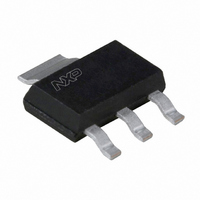
BFG94,115 NXP Semiconductors, BFG94,115 Datasheet - Page 5

BFG94,115
Manufacturer Part Number
BFG94,115
Description
TRANS NPN 10V 60MA SOT223
Manufacturer
NXP Semiconductors
Datasheet
1.BFG94115.pdf
(13 pages)
Specifications of BFG94,115
Package / Case
SOT-223 (3 leads + Tab), SC-73, TO-261
Transistor Type
NPN
Voltage - Collector Emitter Breakdown (max)
12V
Frequency - Transition
6GHz
Noise Figure (db Typ @ F)
2.7dB ~ 3dB @ 500MHz ~ 1GHz
Power - Max
700mW
Dc Current Gain (hfe) (min) @ Ic, Vce
45 @ 30mA, 5V
Current - Collector (ic) (max)
60mA
Mounting Type
Surface Mount
Dc Current Gain Hfe Max
45
Mounting Style
SMD/SMT
Configuration
Single
Transistor Polarity
NPN
Maximum Operating Frequency
4000 MHz
Collector- Emitter Voltage Vceo Max
12 V
Emitter- Base Voltage Vebo
2 V
Continuous Collector Current
0.06 A
Power Dissipation
700 mW
Maximum Operating Temperature
+ 175 C
Lead Free Status / RoHS Status
Lead free / RoHS Compliant
Gain
-
Lead Free Status / RoHS Status
Lead free / RoHS Compliant, Lead free / RoHS Compliant
Other names
934002270115
BFG94 T/R
BFG94 T/R
BFG94 T/R
BFG94 T/R
Philips Semiconductors
September 1995
handbook, halfpage
NPN 6 GHz wideband transistor
V BB
L1 = L3 = 5 H micro-choke.
L2 = 1 turn copper wire (0.4 mm), internal diameter 4 mm.
Fig.2
input
75
(mW)
P tot
800
600
400
200
0
0
Test circuit for second and third order
intermodulation distortion.
1 nF
Fig.4 Power derating curve.
L1
50
2 pF
10 k
33
247
100
L2
1 nF
L3
150
DUT
33
T s ( C)
1 nF
MBB790
200
MBB780
output
75
V CC
5
handbook, halfpage
Fig.3
V
Fig.5
FIXTURE
CE
TEST
DUT
h FE
= 10 V; T
120
80
40
0
0
Measurement set-up for third order
intercept point and 1 dB gain compression.
DC current gain as a function of collector
current.
j
= 25 C
OUTPUT SLUG TUNER
INPUT SLUG TUNER
10
20
Product specification
BIAS
BIAS
TEE
TEE
I
C
(mA)
MCD087
BFG94
MBB789
output
input
30


