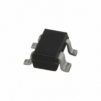
BFG520W/X,115 NXP Semiconductors, BFG520W/X,115 Datasheet - Page 2

BFG520W/X,115
Manufacturer Part Number
BFG520W/X,115
Description
TRANS NPN 70MA 15V 9GHZ SOT343N
Manufacturer
NXP Semiconductors
Specifications of BFG520W/X,115
Package / Case
SOT-343N
Transistor Type
NPN
Voltage - Collector Emitter Breakdown (max)
15V
Frequency - Transition
9GHz
Noise Figure (db Typ @ F)
1.1dB ~ 2.1dB @ 900MHz
Power - Max
500mW
Dc Current Gain (hfe) (min) @ Ic, Vce
60 @ 20mA, 6V
Current - Collector (ic) (max)
70mA
Mounting Type
Surface Mount
Dc Current Gain Hfe Max
60 @ 20mA @ 6V
Mounting Style
SMD/SMT
Configuration
Single Dual Emitter
Transistor Polarity
NPN
Maximum Operating Frequency
9000 MHz (Typ)
Collector- Emitter Voltage Vceo Max
15 V
Emitter- Base Voltage Vebo
2.5 V
Continuous Collector Current
0.07 A
Power Dissipation
500 mW
Maximum Operating Temperature
+ 175 C
Number Of Elements
1
Collector-emitter Voltage
15V
Collector-base Voltage
20V
Emitter-base Voltage
2.5V
Collector Current (dc) (max)
70mA
Dc Current Gain (min)
60
Frequency (max)
9GHz
Operating Temp Range
-65C to 175C
Operating Temperature Classification
Military
Mounting
Surface Mount
Pin Count
3 +Tab
Package Type
SO
Lead Free Status / RoHS Status
Lead free / RoHS Compliant
Gain
-
Lead Free Status / Rohs Status
Lead free / RoHS Compliant
Other names
568-1645-2
934030650115
BFG520W/X T/R
934030650115
BFG520W/X T/R
NXP Semiconductors
FEATURES
APPLICATIONS
RF front end wideband applications in the GHz range,
such as analog and digital cellular telephones, cordless
telephones (CT2, CT3, PCN, DECT, etc.), radar detectors,
pagers, satellite television tuners (SATV) and repeater
amplifiers in fibre-optic systems.
DESCRIPTION
NPN silicon planar epitaxial transistor in a 4-pin
dual-emitter SOT343N plastic package.
MARKING
QUICK REFERENCE DATA
BFG520W
BFG520W/X
V
V
I
P
h
C
f
G
|S
F
TYPE NUMBER
SYMBOL
C
T
FE
High power gain
Low noise figure
High transition frequency
Gold metallization ensures excellent reliability.
CBO
CES
tot
re
NPN 9 GHz wideband transistors
UM
21
|
2
collector-base voltage
collector-emitter voltage R
collector current (DC)
total power dissipation
DC current gain
feedback capacitance
transition frequency
maximum unilateral
power gain
insertion power gain
noise figure
PARAMETER
CODE
N3
N4
open emitter
T
I
I
I
I
I
C
C
C
C
C
s
s
BE
= 20 mA; V
= 0; V
= 20 mA; V
= 20 mA; V
= 20 mA; V
= 0
85 C
opt
Rev. 04 - 21 November 2007
; I
CB
C
= 6 V; f = 1 MHz
= 5 mA; V
CE
CE
CE
CE
= 6 V
= 6 V; f = 1 GHz; T
= 6 V; f = 900 MHz; T
= 6 V; f = 900 MHz; T
CONDITIONS
CE
PINNING
handbook, halfpage
= 6 V; f = 900 MHz
PIN
1
2
3
4
Fig.1 Simplified outline SOT343N.
amb
amb
amb
collector
base
emitter
emitter
= 25 C
BFG520W; BFG520W/X
= 25 C
= 25 C 16
BFG520W
4
1
Top view
DESCRIPTION
60
MIN.
Product specification
3
2
MBK523
120
0.35
9
17
17
1.1
TYP. MAX. UNIT
collector
emitter
base
emitter
BFG520W/X
20
15
70
500
250
1.6
2 of 15
V
V
mA
mW
pF
GHz
dB
dB
dB


