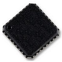
AD5748ACPZ Analog Devices Inc, AD5748ACPZ Datasheet - Page 27

AD5748ACPZ
Manufacturer Part Number
AD5748ACPZ
Description
ZDPLC +/-24V DRIVER
Manufacturer
Analog Devices Inc
Datasheet
1.AD5748ACPZ-RL7.pdf
(32 pages)
Specifications of AD5748ACPZ
Amplifier Type
Instrumentation
Number Of Circuits
1
Slew Rate
2 V/µs
Current - Output / Channel
15mA
Voltage - Supply, Single/dual (±)
±12 V ~ 24 V
Operating Temperature
-40°C ~ 105°C
Mounting Type
Surface Mount
Package / Case
*
No. Of Amplifiers
3
Supply Voltage Range
± 12V To ± 24V
Supply Current
5.2mA
Amplifier Case Style
LFCSP
No. Of Pins
32
Operating Temperature Range
-40°C To +105°C
Svhc
No
Rohs Compliant
Yes
Bandwidth
100kHz
Amplifier Output
Differential
Lead Free Status / RoHS Status
Lead free / RoHS Compliant
Output Type
-
Gain Bandwidth Product
-
-3db Bandwidth
-
Current - Input Bias
-
Voltage - Input Offset
-
Current - Supply
-
Lead Free Status / RoHS Status
Lead free / RoHS Compliant
Readback Operation
Readback mode is activated by selecting the correct device address
(A2, A1, A0) and then setting the R/ W bit to 1. By default, the
SDO pin is disabled. After having addressed the AD5748 for a
read operation, setting R/ W to 1 enables the SDO pin and SDO
data is clocked out on the 5
has been clocked out on SDO, a rising edge on SYNC disables
(tristate) the SDO pin again. Status register data (see
and control register data are both available during the same
read cycle.
The status bits comprise four read-only bits. They are used to
notify the user of specific fault conditions that occur, such as
an open circuit or short circuit on the output, overtemperature
error, or an interface error. If any of these fault conditions occurs,
a hardware FAULT is also asserted low, which can be used as a
hardware interrupt to the controller.
See the Detailed Description of Features section for a full
explanation of fault conditions.
HARDWARE CONTROL
Hardware control is enabled by connecting the HW SELECT
pin to DVCC. In this mode, the R3, R2, R1, and R0 pins in
conjunction with the RSET pin are used to configure the
output range, as per Table 7.
Table 8. Input Shift Register Contents for a Read Operation—Status Register
MSB
D15
A2
Table 9. Status Bit Options
Bit
PEC Error
VOUT Fault
IOUT Fault
OVER TEMP
D14
A1
D13
A0
Description
This bit is set if there is an interface error detected by CRC-8 error checking. See the Detailed Description of Features section.
This bit is set if there is a short circuit on the VOUT pin.
This bit is set is there is an open circuit on the IOUT pin.
This bit is set if the AD5748 core temperature exceeds approximately 150°C.
D12
1
th
rising edge of SCLK. After the data
D11
0
D10
R3
D9
R2
D8
R1
Table 8
D7
R0
)
Rev. A | Page 27 of 32
D6
CLRSEL
D5
OUTEN
In hardware mode, there is no status register. The fault condi-
tions (open circuit, short circuit, and overtemperature) are
available on Pin IFAULT, Pin VFAULT, and Pin TEMP. If any
one of these fault conditions is set, then a low is asserted on the
specific fault pin. IFAULT, VFAULT, and TEMP are open-drain
outputs and, therefore, can be connected together to allow the
user to generate one interrupt to the system controller to commu-
nicate a fault. If hardwired in this way, it is not possible to
isolate which fault occurred in the system.
TRANSFER FUNCTION
The AD5748 consists of an internal signal conditioning block
that maps the analog input voltage to a programmed output
range. The available analog input range is 0 V to 4.096 V.
For all ranges, both current and voltage, the AD5748 imple-
ments a straight linear mapping function. 0 V maps to the
lower end of the selected range; 4.096 V maps to the upper
end of the selected range.
D4
RSET
D3
PEC error
D2
OVER TEMP
D1
IOUT fault
AD5748
LSB
D0
VOUT fault


