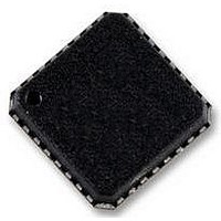
AD5748ACPZ Analog Devices Inc, AD5748ACPZ Datasheet - Page 11

AD5748ACPZ
Manufacturer Part Number
AD5748ACPZ
Description
ZDPLC +/-24V DRIVER
Manufacturer
Analog Devices Inc
Datasheet
1.AD5748ACPZ-RL7.pdf
(32 pages)
Specifications of AD5748ACPZ
Amplifier Type
Instrumentation
Number Of Circuits
1
Slew Rate
2 V/µs
Current - Output / Channel
15mA
Voltage - Supply, Single/dual (±)
±12 V ~ 24 V
Operating Temperature
-40°C ~ 105°C
Mounting Type
Surface Mount
Package / Case
*
No. Of Amplifiers
3
Supply Voltage Range
± 12V To ± 24V
Supply Current
5.2mA
Amplifier Case Style
LFCSP
No. Of Pins
32
Operating Temperature Range
-40°C To +105°C
Svhc
No
Rohs Compliant
Yes
Bandwidth
100kHz
Amplifier Output
Differential
Lead Free Status / RoHS Status
Lead free / RoHS Compliant
Output Type
-
Gain Bandwidth Product
-
-3db Bandwidth
-
Current - Input Bias
-
Voltage - Input Offset
-
Current - Supply
-
Lead Free Status / RoHS Status
Lead free / RoHS Compliant
Pin No.
11
12, 13
14
15
16
17
18
19, 20
21
22
23
24
25, 26,
27, 28
29
30
31
32
33 (EPAD)
Mnemonic
AD0/R3
REXT2, REXT1
VREF
VIN
GND
AVDD
IOUT
COMP2,
COMP1
AVSS
VSENSE−
VOUT
VSENSE+
NC
HW SELECT
RESET
FAULT/TEMP
NC/IFAULT
Exposed
paddle
Description
Device Addressing Bit (AD0). In software mode, this pin, in conjunction with AD1 and AD2, allows up to eight
devices to be addressed on one bus.
Range Decode Bit (R3). In hardware mode, this pin, in conjunction with, R0, R1, and R2, selects the output
current/voltage range setting on the part.
A 15 kΩ external current setting resistor can be connected between the REXT1 and REXT2 pins to improve the
IOUT temperature drift performance.
Buffered Reference Input.
Buffered Analog Input (0 V to 4.096 V).
Ground Connection.
Positive Analog Supply Pin.
Current Output Pin.
Optional Compensation Capacitor Connections for the Voltage Output Buffer. These are used to drive higher
capacitive loads on the output. These pins also reduce overshoot on the output. Care should be taken when
choosing the value of the capacitor connected between the COMP1 and COMP2 pins because it has a direct
influence on the settling time of the output. See the Driving Large Capacitive Loads section for further details.
Negative Analog Supply Pin.
Sense Connection for the Negative Voltage Output Load Connection. This pin must stay within ±3.0 V of
ground for correct operation.
Buffered Analog Output Voltage.
Sense Connection for the Positive Voltage Output Load Connection.
No Connect. Can be tied to GND.
This pin is used to configure the part to hardware or software mode.
HW SELECT = 0 selects software control.
HW SELECT = 1 selects hardware control.
Resets the part to its power-on state.
Fault Alert (FAULT). In software mode, this pin acts as a general fault alert pin. It is asserted low when an open
circuit, short circuit, overtemperature error, or PEC interface error is detected. This pin is an open-drain output
and must be connected to a pull-up resistor.
Overtemperature Fault (TEMP). In hardware mode, this pin acts as an overtemperature fault pin. It is asserted
low when an overtemperature error is detected. This pin is an open-drain output and must be connected to a
pull-up resistor.
No Connect (NC). In software mode, this pin is a no connect. Instead, tie this pin to GND.
Open-Circuit Fault Alert (IFAULT). In hardware mode, this pin acts as an open-circuit fault alert pin. It is asserted
low when an open-circuit error is detected. This pin is an open-drain output and must be connected to a pull-
up resistor.
The exposed paddle is tied to AVSS.
Rev. A | Page 11 of 32
AD5748


