FDP8443 Fairchild Semiconductor, FDP8443 Datasheet - Page 2
FDP8443
Manufacturer Part Number
FDP8443
Description
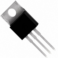
MOSFET N-CH 40V 80A TO-220AB
Manufacturer
Fairchild Semiconductor
Series
PowerTrench®r
Datasheet
1.FDP8443.pdf
(7 pages)
Specifications of FDP8443
Fet Type
MOSFET N-Channel, Metal Oxide
Fet Feature
Logic Level Gate
Rds On (max) @ Id, Vgs
3.5 mOhm @ 80A, 10V
Drain To Source Voltage (vdss)
40V
Current - Continuous Drain (id) @ 25° C
80A
Vgs(th) (max) @ Id
4V @ 250µA
Gate Charge (qg) @ Vgs
185nC @ 10V
Input Capacitance (ciss) @ Vds
9310pF @ 25V
Power - Max
188W
Mounting Type
Through Hole
Package / Case
TO-220-3 (Straight Leads)
Configuration
Single
Transistor Polarity
N-Channel
Resistance Drain-source Rds (on)
0.0035 Ohms
Drain-source Breakdown Voltage
40 V
Gate-source Breakdown Voltage
+/- 20 V
Continuous Drain Current
20 A
Power Dissipation
188 W
Maximum Operating Temperature
+ 175 C
Mounting Style
Through Hole
Minimum Operating Temperature
- 55 C
Lead Free Status / RoHS Status
Lead free / RoHS Compliant
Available stocks
Company
Part Number
Manufacturer
Quantity
Price

Part Number:
FDP8443
Manufacturer:
NXP/µü®µÖ║µĄ”
Quantity:
20 000


FDP8443 Rev. A
Electrical Characteristics
Off Characteristics
On Characteristics
Dynamic Characteristics
MOSFET Maximum Ratings
Thermal Characteristics
Package Marking and Ordering Information
B
I
I
V
r
C
C
C
R
Q
Q
Q
Q
Q
V
V
I
E
P
T
R
R
Symbol
DSS
GSS
DS(on)
Symbol
D
J
VDSS
GS(th)
DSS
GS
AS
D
iss
oss
rss
G
θJC
θJA
g(TOT)
g(TH)
gs
gs2
gd
Device Marking
, T
STG
FDP8443
Thermal Resistance Junction to Case
Thermal Resistance Junction to Ambient
Drain to Source Breakdown Voltage
Zero Gate Voltage Drain Current
Gate to Source Leakage Current
Drain to Source Voltage
Gate to Source Voltage
Drain Current Continuous (T
Continuous (T
Pulsed
Single Pulse Avalanche Energy
Power Dissipation
Derate above 25
Operating and Storage Temperature
Gate to Source Threshold Voltage
Drain to Source On Resistance
Input Capacitance
Output Capacitance
Reverse Transfer Capacitance
Gate Resistance
Total Gate Charge at 10V
Threshold Gate Charge
Gate to Source Gate Charge
Gate Charge Threshold to Plateau
Gate to Drain “Miller“ Charge
amb
Parameter
FDP8443
Device
o
C
= 25
o
C, V
GS
C
= 10V, with R
T
< 144
C
Parameter
TO-220AB
Package
= 25°C unless otherwise noted
T
C
o
= 25°C unless otherwise noted
C, V
V
f = 1MHz
V
V
V
V
I
I
T
I
V
V
V
D
D
GS
D
J
DS
GS
GS
GS
GS
DS
GS
GS
θJA
= 250μA, V
= 80A, V
= 80A, V
= 175
= 10V)
= 25V, V
= 0.5V, f = 1MHz
= 0 to 10V
= 0 to 2V
= 32V,
= V
= 0V
= ±20V
= 62
Test Conditions
DS
2
o
C
o
, I
C/W)
Reel Size
GS
GS
D
GS
GS
Tube
= 10V
= 10V,
= 250μA
= 0V
= 0V,
V
T
I
DD
I
C
g
D
= 150
= 1mA
= 35A
(Note 2)
= 20V
(Note 1)
o
Tape Width
C
N/A
Min
40
2
-
-
-
-
-
-
-
-
-
-
-
-
-
-
See Figure 4
-55 to +175
Ratings
9310
17.5
18.8
800
510
142
Typ
1.25
0.9
0.8
2.8
2.7
4.7
±20
188
36
32
531
62
40
80
20
-
-
-
-
www.fairchildsemi.com
±100
Max
Quantity
250
185
3.5
6.1
23
50 units
1
-
4
-
-
-
-
-
-
-
Units
o
o
Units
W/
μA
nA
mΩ
nC
nC
nC
nC
nC
C/W
C/W
pF
pF
pF
Ω
mJ
V
o
W
V
V
V
A
C
o
C
Related parts for FDP8443
Image
Part Number
Description
Manufacturer
Datasheet
Request
R

Part Number:
Description:
Fairchild Semiconductor [IGBT MODULE]
Manufacturer:
Fairchild Semiconductor
Datasheet:

Part Number:
Description:
Discrete Semiconductor Modules
Manufacturer:
Fairchild Semiconductor
Part Number:
Description:
Discrete Semiconductor Modules
Manufacturer:
Fairchild Semiconductor
Part Number:
Description:
This N-Channel MOSFET is produced using Fairchild SemiconductorÆs advanced Power Trench« process
Manufacturer:
Fairchild Semiconductor
Datasheet:
Part Number:
Description:
This N-Channel MOSFET is produced using Fairchild SemiconductorÆs advanced Power Trench« process
Manufacturer:
Fairchild Semiconductor
Datasheet:
Part Number:
Description:
This N-Channel MOSFET is produced using Fairchild SemiconductorÆs advanced PowerTrench« process
Manufacturer:
Fairchild Semiconductor
Datasheet:
Part Number:
Description:
This N-Channel MOSFET is produced using Fairchild SemiconductorÆs advanced PowerTrench« process
Manufacturer:
Fairchild Semiconductor
Datasheet:
Part Number:
Description:
This N-Channel MOSFET is produced using Fairchild SemiconductorÆs advanced Power Trench« process
Manufacturer:
Fairchild Semiconductor
Datasheet:
Part Number:
Description:
This N-Channel logic Level MOSFETs are produced using Fairchild Semiconductoræs advanced Power Trench« process that has been special tailored to minimize the on-state resistance and yet maintain superior switching performance
Manufacturer:
Fairchild Semiconductor
Datasheet:
Part Number:
Description:
This N-Channel MOSFET is produced using Fairchild SemiconductorÆs advanced Power Trench« process
Manufacturer:
Fairchild Semiconductor
Datasheet:
Part Number:
Description:
This N-Channel SyncFETÖ is produced using Fairchild SemiconductorÆs advanced PowerTrench« process
Manufacturer:
Fairchild Semiconductor
Datasheet:
Part Number:
Description:
This N-Channel SyncFETÖ is produced using Fairchild SemiconductorÆs advanced PowerTrench« process
Manufacturer:
Fairchild Semiconductor
Datasheet:
Part Number:
Description:
This N-Channel SyncFETÖ is produced using Fairchild SemiconductorÆs advanced PowerTrench« process
Manufacturer:
Fairchild Semiconductor
Datasheet:
Part Number:
Description:
This N-Channel logic Level MOSFETs are produced using Fairchild Semiconductoræs advanced Power Trench« process that has been special tailored to minimize the on-state resistance and yet maintain superior switching performance
Manufacturer:
Fairchild Semiconductor
Datasheet:
Part Number:
Description:
This N-Channel MOSFET is produced using Fairchild SemiconductorÆs advanced Power Trench« process that has been especially tailored to minimize the on-state resistance and yet maintain superior switching performance
Manufacturer:
Fairchild Semiconductor
Datasheet: