FDA70N20 Fairchild Semiconductor, FDA70N20 Datasheet - Page 2
FDA70N20
Manufacturer Part Number
FDA70N20
Description
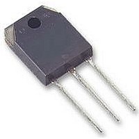
MOSFET N-CH 200V 70A TO-3P
Manufacturer
Fairchild Semiconductor
Series
UniFET™r
Datasheet
1.FDA70N20.pdf
(8 pages)
Specifications of FDA70N20
Fet Type
MOSFET N-Channel, Metal Oxide
Fet Feature
Standard
Rds On (max) @ Id, Vgs
35 mOhm @ 35A, 10V
Drain To Source Voltage (vdss)
200V
Current - Continuous Drain (id) @ 25° C
70A
Vgs(th) (max) @ Id
5V @ 250µA
Gate Charge (qg) @ Vgs
86nC @ 10V
Input Capacitance (ciss) @ Vds
3970pF @ 25V
Power - Max
417W
Mounting Type
Through Hole
Package / Case
TO-3PN-3
Transistor Polarity
N Channel
Continuous Drain Current Id
70A
Drain Source Voltage Vds
200V
On Resistance Rds(on)
35mohm
Rds(on) Test Voltage Vgs
10V
Threshold Voltage Vgs Typ
5V
Rohs Compliant
Yes
Configuration
Single
Resistance Drain-source Rds (on)
0.035 Ohms
Drain-source Breakdown Voltage
200 V
Gate-source Breakdown Voltage
+/- 30 V
Continuous Drain Current
70 A
Power Dissipation
417 W
Maximum Operating Temperature
+ 150 C
Mounting Style
Through Hole
Minimum Operating Temperature
- 55 C
Lead Free Status / RoHS Status
Lead free / RoHS Compliant
Available stocks
Company
Part Number
Manufacturer
Quantity
Price
Company:

Part Number:
FDA70N20
Manufacturer:
ST
Quantity:
5 000


FDA70N20 Rev. A
Package Marking and Ordering Information
Electrical Characteristics
NOTES:
1. Repetitive Rating: Pulse width limited by maximum junction temperature
2. L = 0.533mH, I
3. I
4. Pulse Test: Pulse width ≤ 300µs, Duty Cycle ≤ 2%
5. Essentially Independent of Operating Temperature Typical Characteristics
Off Characteristics
BV
∆BV
/
I
I
I
On Characteristics
V
R
g
Dynamic Characteristics
C
C
C
Switching Characteristics
t
t
t
t
Q
Q
Q
Drain-Source Diode Characteristics and Maximum Ratings
I
I
V
t
Q
Device Marking
Symbol
DSS
GSSF
GSSR
d(on)
r
d(off)
f
S
SM
rr
FS
GS(th)
SD
SD
DS(on)
iss
oss
rss
g
gs
gd
rr
DSS
∆T
≤ 70A, di/dt ≤ 200A/µs, V
DSS
FDA70N20
J
AS
Drain-Source Breakdown Voltage
Breakdown Voltage Temperature
Coefficient
Zero Gate Voltage Drain Current
Gate-Body Leakage Current, Forward
Gate-Body Leakage Current, Reverse
Gate Threshold Voltage
Static Drain-Source
On-Resistance
Forward Transconductance
Input Capacitance
Output Capacitance
Reverse Transfer Capacitance
Turn-On Delay Time
Turn-On Rise Time
Turn-Off Delay Time
Turn-Off Fall Time
Total Gate Charge
Gate-Source Charge
Gate-Drain Charge
Maximum Continuous Drain-Source Diode Forward Current
Maximum Pulsed Drain-Source Diode Forward Current
Drain-Source Diode Forward Voltage
Reverse Recovery Time
Reverse Recovery Charge
= 70A, V
DD
DD
= 50V, R
≤ BV
Parameter
FDA70N20
Device
DSS
G
= 25Ω, Starting T
, Starting T
J
= 25°C
T
C
= 25°C unless otherwise noted
J
= 25°C
Package
TO-3PN
V
I
V
V
V
V
V
V
V
V
f = 1.0MHz
V
R
V
V
V
V
dI
D
GS
DS
DS
GS
GS
DS
GS
DS
DS
DD
DS
GS
GS
GS
G
F
= 250µA, Referenced to 25°C
/dt =100A/µs
= 25Ω
= 200V, V
= 160V, T
= V
= 40V, I
= 25V, V
= 160V, I
= 0V, I
= 30V, V
= -30V, V
= 10V, I
= 100V, I
= 10V
= 0V, I
= 0V, I
GS
2
, I
D
S
S
D
D
D
Conditions
= 70A
= 70A
= 250µA
DS
GS
D
D
DS
= 35A
GS
C
= 35A
= 250µA
= 70A
= 70A
Reel Size
= 125°C
= 0V
= 0V,
= 0V
= 0V
-
(Note 4, 5)
(Note 4, 5)
(Note 4)
(Note 4)
Tape Width
Min.
200
3.0
-
--
--
--
--
--
--
--
--
--
--
--
--
--
--
--
--
--
--
--
--
--
--
Typ.
0.029
3050
750
235
175
0.2
4.1
89
47
71
65
39
66
19
26
--
--
--
--
--
--
--
--
--
Quantity
0.035
Max Units
3970
-100
www.fairchildsemi.com
100
980
130
150
480
140
280
5.0
1.4
70
10
88
86
--
--
1
--
--
--
--
--
30
V/°C
nC
nC
nC
µC
µA
µA
nA
nA
pF
pF
pF
ns
ns
ns
ns
ns
V
V
Ω
S
A
A
V
Related parts for FDA70N20
Image
Part Number
Description
Manufacturer
Datasheet
Request
R

Part Number:
Description:
Fairchild Semiconductor [IGBT MODULE]
Manufacturer:
Fairchild Semiconductor
Datasheet:

Part Number:
Description:
Discrete Semiconductor Modules
Manufacturer:
Fairchild Semiconductor
Part Number:
Description:
Discrete Semiconductor Modules
Manufacturer:
Fairchild Semiconductor
Part Number:
Description:
This N-Channel MOSFET is produced using Fairchild Semiconductor’s advanced Power Trench® process
Manufacturer:
Fairchild Semiconductor
Datasheet:
Part Number:
Description:
This N-Channel MOSFET is produced using Fairchild Semiconductor’s advanced Power Trench® process
Manufacturer:
Fairchild Semiconductor
Datasheet:
Part Number:
Description:
This N-Channel MOSFET is produced using Fairchild Semiconductor’s advanced PowerTrench® process
Manufacturer:
Fairchild Semiconductor
Datasheet:
Part Number:
Description:
This N-Channel MOSFET is produced using Fairchild Semiconductor’s advanced PowerTrench® process
Manufacturer:
Fairchild Semiconductor
Datasheet:
Part Number:
Description:
This N-Channel MOSFET is produced using Fairchild Semiconductor’s advanced Power Trench® process
Manufacturer:
Fairchild Semiconductor
Datasheet:
Part Number:
Description:
This N-Channel logic Level MOSFETs are produced using Fairchild Semiconductor‘s advanced Power Trench® process that has been special tailored to minimize the on-state resistance and yet maintain superior switching performance
Manufacturer:
Fairchild Semiconductor
Datasheet:
Part Number:
Description:
This N-Channel MOSFET is produced using Fairchild Semiconductor’s advanced Power Trench® process
Manufacturer:
Fairchild Semiconductor
Datasheet:
Part Number:
Description:
This N-Channel SyncFET™ is produced using Fairchild Semiconductor’s advanced PowerTrench® process
Manufacturer:
Fairchild Semiconductor
Datasheet:
Part Number:
Description:
This N-Channel SyncFET™ is produced using Fairchild Semiconductor’s advanced PowerTrench® process
Manufacturer:
Fairchild Semiconductor
Datasheet:
Part Number:
Description:
This N-Channel SyncFET™ is produced using Fairchild Semiconductor’s advanced PowerTrench® process
Manufacturer:
Fairchild Semiconductor
Datasheet:
Part Number:
Description:
This N-Channel logic Level MOSFETs are produced using Fairchild Semiconductor‘s advanced Power Trench® process that has been special tailored to minimize the on-state resistance and yet maintain superior switching performance
Manufacturer:
Fairchild Semiconductor
Datasheet:
Part Number:
Description:
This N-Channel MOSFET is produced using Fairchild Semiconductor’s advanced Power Trench® process that has been especially tailored to minimize the on-state resistance and yet maintain superior switching performance
Manufacturer:
Fairchild Semiconductor
Datasheet: