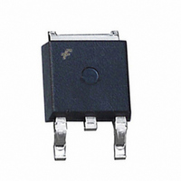
FDD2670 Fairchild Semiconductor, FDD2670 Datasheet - Page 3

FDD2670
Manufacturer Part Number
FDD2670
Description
MOSFET N-CH 200V 3.6A D-PAK
Manufacturer
Fairchild Semiconductor
Series
PowerTrench®r
Datasheet
1.FDD2670.pdf
(5 pages)
Specifications of FDD2670
Fet Type
MOSFET N-Channel, Metal Oxide
Fet Feature
Standard
Rds On (max) @ Id, Vgs
130 mOhm @ 3.6A, 10V
Drain To Source Voltage (vdss)
200V
Current - Continuous Drain (id) @ 25° C
3.6A
Vgs(th) (max) @ Id
4.5V @ 250µA
Gate Charge (qg) @ Vgs
43nC @ 10V
Input Capacitance (ciss) @ Vds
1228pF @ 100V
Power - Max
1.3W
Mounting Type
Surface Mount
Package / Case
DPak, TO-252 (2 leads+tab), SC-63
Transistor Polarity
N Channel
Continuous Drain Current Id
3.6A
Drain Source Voltage Vds
200V
On Resistance Rds(on)
130mohm
Rds(on) Test Voltage Vgs
10V
Threshold Voltage Vgs Typ
4V
Rohs Compliant
Yes
Configuration
Single
Resistance Drain-source Rds (on)
0.13 Ohms
Forward Transconductance Gfs (max / Min)
15 S
Drain-source Breakdown Voltage
200 V
Gate-source Breakdown Voltage
+/- 20 V
Continuous Drain Current
3.6 A
Power Dissipation
3.2 W
Maximum Operating Temperature
+ 150 C
Mounting Style
SMD/SMT
Minimum Operating Temperature
- 55 C
Lead Free Status / RoHS Status
Lead free / RoHS Compliant
Available stocks
Company
Part Number
Manufacturer
Quantity
Price
Part Number:
FDD2670
Manufacturer:
FAIRCHILD/仙童
Quantity:
20 000
Typical Characteristics
30
24
18
12
6
0
20
15
10
5
0
Figure 3. On-Resistance Variation with
2.5
1.5
0.5
3
Figure 1. On-Region Characteristics.
0
2
1
0
-50
Figure 5. Transfer Characteristics.
V
GS
V
= 10V
V
I
D
GS
DS
= 3.6A
-25
= 10V
= 15V
4
2
V
GS
V
T
, GATE TO SOURCE VOLTAGE (V)
6.5V
0
DS
J
, JUNCTION TEMPERATURE (
Temperature.
, DRAIN-SOURCE VOLTAGE (V)
T
A
= 125
25
5
4
o
C
6.0V
25
50
o
C
6
-55
6
75
o
C
5.5V
100
o
C)
7
8
125
150
8
10
Figure 6. Body Diode Forward Voltage Variation
0.4
0.3
0.2
0.1
0.001
0
0.01
100
0.1
4
10
1.6
1.4
1.2
0.8
Figure 2. On-Resistance Variation with
Figure 4. On-Resistance Variation with
with Source Current and Temperature.
1
1
0
0
V
Drain Current and Gate Voltage.
V
GS
GS
= 0V
= 5.5V
5
0.2
Gate-to-Source Voltage.
V
SD
V
4
GS
, BODY DIODE FORWARD VOLTAGE (V)
, GATE TO SOURCE VOLTAGE (V)
0.4
T
6
A
= 125
I
D
T
, DRAIN CURRENT (A)
A
= 125
o
8
0.6
C
T
A
7
6.0V
o
C
25
= 25
o
C
0.8
o
C
12
-55
8
6.5V
o
C
1
FDD2670 Rev C1(W)
16
I
9
D
1.2
= 1.8 A
10.0V
1.4
10
20


