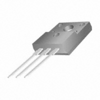
FQPF15P12 Fairchild Semiconductor, FQPF15P12 Datasheet - Page 3

FQPF15P12
Manufacturer Part Number
FQPF15P12
Description
MOSFET P-CH 120V 15A TO-220F
Manufacturer
Fairchild Semiconductor
Series
QFET™r
Datasheet
1.FQPF15P12.pdf
(10 pages)
Specifications of FQPF15P12
Fet Type
MOSFET P-Channel, Metal Oxide
Fet Feature
Standard
Rds On (max) @ Id, Vgs
200 mOhm @ 7.5A, 10V
Drain To Source Voltage (vdss)
120V
Current - Continuous Drain (id) @ 25° C
15A
Vgs(th) (max) @ Id
4V @ 250µA
Gate Charge (qg) @ Vgs
38nC @ 10V
Input Capacitance (ciss) @ Vds
1100pF @ 25V
Power - Max
41W
Mounting Type
Through Hole
Package / Case
TO-220-3 Full Pack (Straight Leads)
Configuration
Single
Transistor Polarity
P-Channel
Resistance Drain-source Rds (on)
0.2 Ohms
Forward Transconductance Gfs (max / Min)
9.5 S
Drain-source Breakdown Voltage
- 120 V
Gate-source Breakdown Voltage
+/- 30 V
Continuous Drain Current
15 A
Power Dissipation
41 W
Maximum Operating Temperature
+ 175 C
Mounting Style
Through Hole
Minimum Operating Temperature
- 55 C
Lead Free Status / RoHS Status
Lead free / RoHS Compliant
Available stocks
Company
Part Number
Manufacturer
Quantity
Price
Company:
Part Number:
FQPF15P12
Manufacturer:
FAIRCHILD
Quantity:
12 500
©2003 Fairchild Semiconductor Corporation
Typical Characteristics
1.0
0.9
0.8
0.7
0.6
0.5
0.4
0.3
0.2
0.1
0.0
2200
2000
1800
1600
1400
1200
1000
10
10
10
10
800
600
400
200
-1
2
1
0
10
0
0
10
-1
Top :
Bottom : -4.5 V
-1
Figure 5. Capacitance Characteristics
Figure 3. On-Resistance Variation vs
Figure 1. On-Region Characteristics
Drain Current and Gate Voltage
-10.0 V
-15.0 V
-8.0 V
-7.0 V
-6.0 V
-5.5 V
-5.0 V
V
GS
C
oss
C
-V
iss
-V
C
DS
DS
20
rss
, Drain-Source Voltage [V]
-I
, Drain-Source Voltage [V]
D
10
10
, Drain Current [A]
0
0
V
GS
= -10V
40
C
C
C
iss
oss
rss
= C
= C
= C
10
※ Notes :
※ Note : T
gs
gd
ds
10
1. 250μ s Pulse Test
2. T
1
+ C
+ C
1
C
gd
V
gd
= 25℃
GS
(C
※ Notes ;
1. V
2. f = 1 MHz
ds
J
= -20V
= 25℃
= shorted)
GS
= 0 V
60
10
10
12
10
10
10
10
10
10
8
6
4
2
0
-1
-1
2
1
0
1
0
0.0
0
2
Figure 4. Body Diode Forward Voltage
25
Figure 6. Gate Charge Characteristics
o
C
Figure 2. Transfer Characteristics
175
0.5
175℃
Variation with Source Current
o
C
25℃
10
1.0
V
4
DS
-V
-V
Q
V
and Temperature
= -96V
-55
GS
SD
DS
G
V
, Total Gate Charge [nC]
, Gate-Source Voltage [V]
, Source-Drain voltage [V]
o
= -60V
C
DS
1.5
= -30V
2.0
20
6
2.5
※ Notes :
※ Notes :
1. V
2. 250μ s Pulse Test
1. V
2. 250μ s Pulse Test
3.0
※ Note : I
30
8
DS
GS
= -40V
= 0V
D
3.5
= -15A
Rev. A, December 2003
4.0
10
40


