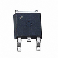
FDD4141 Fairchild Semiconductor, FDD4141 Datasheet - Page 4

FDD4141
Manufacturer Part Number
FDD4141
Description
MOSFET P-CH 40V 10.8A DPAK
Manufacturer
Fairchild Semiconductor
Series
PowerTrench®r
Type
Power MOSFETr
Datasheet
1.FDD4141.pdf
(6 pages)
Specifications of FDD4141
Fet Type
MOSFET P-Channel, Metal Oxide
Fet Feature
Logic Level Gate
Rds On (max) @ Id, Vgs
12.3 mOhm @ 12.7A, 10V
Drain To Source Voltage (vdss)
40V
Current - Continuous Drain (id) @ 25° C
10.8A
Vgs(th) (max) @ Id
3V @ 250µA
Gate Charge (qg) @ Vgs
50nC @ 10V
Input Capacitance (ciss) @ Vds
2775pF @ 20V
Power - Max
2.4W
Mounting Type
Surface Mount
Package / Case
DPak, TO-252 (2 leads+tab), SC-63
Configuration
Single
Transistor Polarity
P-Channel
Resistance Drain-source Rds (on)
12.3 Ohm @ 10 V
Drain-source Breakdown Voltage
40 V
Gate-source Breakdown Voltage
+/- 20 V
Continuous Drain Current
10.8 A
Power Dissipation
2400 mW
Maximum Operating Temperature
+ 150 C
Mounting Style
SMD/SMT
Minimum Operating Temperature
- 55 C
Number Of Elements
1
Polarity
P
Channel Mode
Enhancement
Drain-source On-res
12.3Ohm
Drain-source On-volt
40V
Gate-source Voltage (max)
±20V
Operating Temp Range
-55C to 150C
Operating Temperature Classification
Military
Mounting
Surface Mount
Pin Count
2 +Tab
Package Type
TO-252
Lead Free Status / RoHS Status
Lead free / RoHS Compliant
Other names
FDD4141
FDD4141TR
FDD4141TR
Available stocks
Company
Part Number
Manufacturer
Quantity
Price
Company:
Part Number:
FDD4141
Manufacturer:
Fairchild Semiconductor
Quantity:
33 824
Part Number:
FDD4141
Manufacturer:
FAIRCHILD/仙童
Quantity:
20 000
Part Number:
FDD4141-F085
Manufacturer:
ON/安森美
Quantity:
20 000
©2007 Fairchild Semiconductor Corporation
FDD4141 Rev.C
Typical Characteristics
Figure 7.
200
100
0.1
30
10
10
10
1
1
8
6
4
2
0
0.01
0.1
Figure 9.
0
Figure 11. Forward Bias Safe
THIS AREA IS
LIMITED BY r
I
D
= -12.7A
Switching Capability
Gate Charge Characteristics
-V
0.1
V
8
Operating Area
DS
Unclamped Inductive
DD
t
AV
, DRAIN to SOURCE VOLTAGE (V)
DS(on)
= -10V
, TIME IN AVALANCHE(ms)
Q
SINGLE PULSE
T
R
T
J
C
g
T
θ
1
, GATE CHARGE(nC)
JC
J
= MAX RATED
V
= 25
= 125
DD
= 1.8
16
1
o
= -15V
C
o
o
C
C/W
T
J
10
= 25°C unless otherwise noted
24
V
10
DD
T
J
= -20V
= 25
100
o
32
C
100us
10ms
1ms
DC
1000
100
40
4
10000
10000
1000
1000
100
100
60
50
40
30
20
10
50
Figure 10.
25
10
0
0.1
Figure 12.
-5
Limited by Package
R
Figure 8.
Current vs Case Temperature
θ
f = 1MHz
V
JC
10
GS
= 1.8
-4
V
= 0V
50
V
GS
-V
GS
Power Dissipation
Maximum Continuous Drain
10
DS
o
to Source Voltage
= -4.5V
C/W
T
= -10V
, DRAIN TO SOURCE VOLTAGE (V)
-3
C
Single Pulse Maximum
Capacitance vs Drain
,
t, PULSE WIDTH (s)
CASE TEMPERATURE (
10
75
1
-2
10
FOR TEMPERATURES
ABOVE 25
CURRENT AS FOLLOWS:
-1
I = I
100
25
10
0
SINGLE PULSE
R
o
C DERATE PEAK
θ
150 T
------------------------
JC
C
C
C
V
10
o
iss
oss
rss
125
C )
= 1.8
GS
125
10
–
1
= -10V
www.fairchildsemi.com
C
T
o
C
C/W
10
= 25
2
o
150
C
10
40
3


