FDD4141 Fairchild Semiconductor, FDD4141 Datasheet
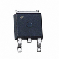
MOSFET P-CH 40V 10.8A DPAK

FDD4141

Manufacturer Part Number
FDD4141
Description
MOSFET P-CH 40V 10.8A DPAK
Manufacturer
Fairchild Semiconductor
Series
PowerTrench®r
Type
Power MOSFETr
Datasheet

Specifications of FDD4141

Fet Type
MOSFET P-Channel, Metal Oxide
Fet Feature
Logic Level Gate
Rds On (max) @ Id, Vgs
12.3 mOhm @ 12.7A, 10V
Drain To Source Voltage (vdss)
40V
Current - Continuous Drain (id) @ 25° C
10.8A
Vgs(th) (max) @ Id
3V @ 250µA
Gate Charge (qg) @ Vgs
50nC @ 10V
Input Capacitance (ciss) @ Vds
2775pF @ 20V
Power - Max
2.4W
Mounting Type
Surface Mount
Package / Case
DPak, TO-252 (2 leads+tab), SC-63
Configuration
Single
Transistor Polarity
P-Channel
Resistance Drain-source Rds (on)
12.3 Ohm @ 10 V
Drain-source Breakdown Voltage
40 V
Gate-source Breakdown Voltage
+/- 20 V
Continuous Drain Current
10.8 A
Power Dissipation
2400 mW
Maximum Operating Temperature
+ 150 C
Mounting Style
SMD/SMT
Minimum Operating Temperature
- 55 C
Number Of Elements
1
Polarity
P
Channel Mode
Enhancement
Drain-source On-res
12.3Ohm
Drain-source On-volt
40V
Gate-source Voltage (max)
±20V
Operating Temp Range
-55C to 150C
Operating Temperature Classification
Military
Mounting
Surface Mount
Pin Count
2 +Tab
Package Type
TO-252
Lead Free Status / RoHS Status
Lead free / RoHS Compliant
Other names
FDD4141
FDD4141TR

Available stocks

Company
Part Number
Manufacturer
Quantity
Price
Part Number:
FDD4141
Manufacturer:
Fairchild Semiconductor
Quantity:
33 824
Part Number:
FDD4141
Manufacturer:
FAIRCHILD/仙童
Quantity:
20 000
Part Number:
FDD4141
0
Company:
Part Number:
FDD4141
Quantity:
5 000
Part Number:
FDD4141-F085
Manufacturer:
ON/安森美
Quantity:
20 000
Part Number:
FDD4141-F085
0
Company:
Part Number:
FDD4141-F085
Quantity:
12 000
©2007 Fairchild Semiconductor Corporation
FDD4141 Rev.C
FDD4141
P-Channel PowerTrench
-40V, -50A, 12.3mΩ
Features
MOSFET Maximum Ratings
Thermal Characteristics
Package Marking and Ordering Information
V
V
I
E
P
T
R
R
D
DS
GS
AS
D
J
θJC
θJA
Max r
Max r
High performance trench technology for extremely low r
RoHS Compliant
, T
Symbol
Device Marking
STG
FDD4141
DS(on)
DS(on)
= 12.3mΩ at V
= 18.0mΩ at V
Drain to Source Voltage
Gate to Source Voltage
Drain Current -Continuous (Package limited)
Single Pulse Avalanche Energy
Power Dissipation
Power Dissipation
Operating and Storage Junction Temperature Range
Thermal Resistance, Junction to Case
Thermal Resistance, Junction to Ambient
G
S
GS
GS
= -10V, I
= -4.5V, I
(TO -252)
-Continuous
-Continuous (Silicon limited)
-Pulsed
FDD4141
D -PA K
Device
TO -2 52
D
D
= -12.7A
= -10.4A
T
®
C
= 25°C unless otherwise noted
D
MOSFET
Parameter
D-PAK (TO-252)
DS(on)
Package
1
T
T
T
T
T
General Description
This P-Channel MOSFET has been produced using Fairchild
Semiconductor’s proprietary PowerTrench
deliver low r
superior performance benefit in the applications. and optimized
switching performance capability reducing power dissipation
losses in converter/inverter applications.
Applications
C
C
C
A
A
= 25°C
= 25°C
= 25°C
= 25°C
= 25°C
Inverter
Power Supplies
Reel Size
DS(on)
13’’
(Note 1a)
(Note 1a)
(Note 1a)
(Note 3)
G
and optimized Bvdss capability to offer
Tape Width
S
D
12mm
-55 to +150
Ratings
-10.8
-100
±20
337
-40
-50
-58
2.4
1.8
69
52
®
July 2007
technology to
www.fairchildsemi.com
2500 units
Quantity
Units
°C/W
mJ
°C
W
V
V
A
tm

Related parts for FDD4141

FDD4141 Summary of contents

Page 1

... R Thermal Resistance, Junction to Ambient θJA Package Marking and Ordering Information Device Marking Device FDD4141 FDD4141 ©2007 Fairchild Semiconductor Corporation FDD4141 Rev.C ® MOSFET General Description = -12.7A This P-Channel MOSFET has been produced using Fairchild D Semiconductor’s proprietary PowerTrench = -10.4A D deliver low r superior performance benefit in the applications ...

Page 2

... Pulse Test: Pulse Width < 300µs, Duty cycle < 2.0%. ° 3: Starting 3mH 15A ©2007 Fairchild Semiconductor Corporation FDD4141 Rev 25°C unless otherwise noted J Test Conditions I = -250µ -250µA, referenced to 25° -32V, V ...

Page 3

... PULSE DURATION = 80 s DUTY CYCLE = 0.5%MAX - 150 GATE TO SOURCE VOLTAGE (V) GS Figure 5. Transfer Characteristics ©2007 Fairchild Semiconductor Corporation FDD4141 Rev 25°C unless otherwise noted J 4.0 µ PULSE DURATION = 80 s 3.5 DUTY CYCLE = 0.5%MAX 3 -4V GS 2.5 2 -3.5V GS 1.5 1 - 100 125 150 ...

Page 4

... THIS AREA IS LIMITED BY r DS(on) 1 SINGLE PULSE T = MAX RATED 1.8 θ 0.1 0 DRAIN to SOURCE VOLTAGE (V) DS Figure 11. Forward Bias Safe Operating Area ©2007 Fairchild Semiconductor Corporation FDD4141 Rev 25°C unless otherwise noted J 10000 V = -20V DD 1000 100 1000 10000 100us 1000 1ms 10ms DC ...

Page 5

... Typical Characteristics 2 1 DUTY CYCLE-DESCENDING ORDER D = 0.5 0.2 0.1 0.05 0.02 0.1 0.01 SINGLE PULSE 0. 1.8 C/W θ JC 0.005 - ©2007 Fairchild Semiconductor Corporation FDD4141 Rev 25°C unless otherwise noted RECTANGULAR PULSE DURATION (s) Figure 13. Transient Thermal Response Curve NOTES: DUTY FACTOR PEAK ...

Page 6

... PRODUCT STATUS DEFINITIONS Definition of Terms Datasheet Identification Advance Information Preliminary No Identification Needed Obsolete ©2007 Fairchild Semiconductor Corporation FDD4141 Rev.C Green FPS™ e-Series™ POWEREDGE GOT™ Power-SPM™ i-Lo™ PowerTrench IntelliMAX™ Programmable Active Droop™ ...

Related keywords