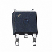
FQD12N20LTM Fairchild Semiconductor, FQD12N20LTM Datasheet - Page 4

FQD12N20LTM
Manufacturer Part Number
FQD12N20LTM
Description
MOSFET N-CH 200V 9A DPAK
Manufacturer
Fairchild Semiconductor
Series
QFET™r
Specifications of FQD12N20LTM
Fet Type
MOSFET N-Channel, Metal Oxide
Fet Feature
Logic Level Gate
Rds On (max) @ Id, Vgs
280 mOhm @ 4.5A, 10V
Drain To Source Voltage (vdss)
200V
Current - Continuous Drain (id) @ 25° C
9A
Vgs(th) (max) @ Id
2V @ 250µA
Gate Charge (qg) @ Vgs
21nC @ 5V
Input Capacitance (ciss) @ Vds
1080pF @ 25V
Power - Max
2.5W
Mounting Type
Surface Mount
Package / Case
DPak, TO-252 (2 leads+tab), SC-63
Configuration
Single
Transistor Polarity
N-Channel
Resistance Drain-source Rds (on)
0.28 Ohm @ 10 V
Forward Transconductance Gfs (max / Min)
11.6 S
Drain-source Breakdown Voltage
200 V
Gate-source Breakdown Voltage
+/- 20 V
Continuous Drain Current
9 A
Power Dissipation
2500 mW
Maximum Operating Temperature
+ 150 C
Mounting Style
SMD/SMT
Minimum Operating Temperature
- 55 C
Lead Free Status / RoHS Status
Lead free / RoHS Compliant
Other names
FQD12N20LTM
FQD12N20LTMTR
FQD12N20LTMTR
Available stocks
Company
Part Number
Manufacturer
Quantity
Price
Part Number:
FQD12N20LTM
Manufacturer:
FAIRCHILD/仙童
Quantity:
20 000
©2009 Fairchild Semiconductor Corporation
Typical Characteristics
10
1.2
1.1
1.0
0.9
0.8
10
10
10
Figure 9. Maximum Safe Operating Area
-100
-1
2
1
0
10
Figure 7. Breakdown Voltage Variation
0
-50
T
Operation in This Area
is Limited by R
V
vs. Temperature
J
DS
, Junction Temperature [
, Drain-Source Voltage [V]
0
1 0
※ Notes :
1 0
10
1. T
2. T
3. Single Pulse
1
- 1
1 0
0
C
J
= 150
= 25
DS(on)
- 5
DC
D = 0 . 5
o
0 .0 5
0 .0 2
0 .0 1
C
o
0 .1
50
C
0 .2
10 ms
Figure 11. Transient Thermal Response Curve
1 ms
100
1 0
(Continued)
o
100 s
- 4
C]
s in g le p u ls e
10
※ Notes :
1. V
2. I
t
2
1
, S q u a r e W a v e P u ls e D u r a t io n [ s e c ]
D
GS
= 250 μ A
150
10 s
= 0 V
1 0
- 3
200
1 0
- 2
9.0
7.5
6.0
4.5
3.0
1.5
0.0
3.0
2.5
2.0
1.5
1.0
0.5
0.0
-100
25
Figure 8. On-Resistance Variation
※ N o te s :
Figure 10. Maximum Drain Current
1 0
1 . Z
2 . D u ty F a c t o r , D = t
3 . T
- 1
P
DM
-50
θ J C
J M
50
- T
( t ) = 2 . 2 7 ℃ /W M a x .
vs. Case Temperature
C
= P
T
vs. Temperature
T
t
J
1
, Junction Temperature [
C
D M
t
0
, Case Temperature [ ℃ ]
1 0
2
* Z
0
75
1
θ J C
/t
2
( t )
50
100
1 0
1
100
o
C]
125
※ Notes :
1. V
2. I
150
D
GS
= 5.8 A
= 10 V
Rev. A2, January 2009
200
150


