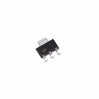
STN1N20 STMicroelectronics, STN1N20 Datasheet - Page 3

STN1N20
Manufacturer Part Number
STN1N20
Description
MOSFET N-CH 200V 1A SOT223
Manufacturer
STMicroelectronics
Specifications of STN1N20
Fet Type
MOSFET N-Channel, Metal Oxide
Fet Feature
Logic Level Gate
Rds On (max) @ Id, Vgs
1.5 Ohm @ 500mA, 10V
Drain To Source Voltage (vdss)
200V
Current - Continuous Drain (id) @ 25° C
1A
Vgs(th) (max) @ Id
5V @ 250µA
Gate Charge (qg) @ Vgs
15.7nC @ 10V
Input Capacitance (ciss) @ Vds
206pF @ 25V
Power - Max
2.9W
Mounting Type
Surface Mount
Package / Case
SOT-223 (3 leads + Tab), SC-73, TO-261
Configuration
Single Dual Drain
Transistor Polarity
N-Channel
Resistance Drain-source Rds (on)
1.5 Ohms
Forward Transconductance Gfs (max / Min)
0.7 S
Drain-source Breakdown Voltage
200 V
Gate-source Breakdown Voltage
+/- 20 V
Continuous Drain Current
1 A
Power Dissipation
2.9 W
Maximum Operating Temperature
+ 150 C
Mounting Style
SMD/SMT
Minimum Operating Temperature
- 55 C
Continuous Drain Current Id
1A
Drain Source Voltage Vds
200V
On Resistance Rds(on)
1.5ohm
Rds(on) Test Voltage Vgs
10V
Threshold Voltage Vgs Typ
3V
Rohs Compliant
Yes
Lead Free Status / RoHS Status
Lead free / RoHS Compliant
Other names
497-3176-2
Available stocks
Company
Part Number
Manufacturer
Quantity
Price
Company:
Part Number:
STN1N20
Manufacturer:
ST MICROELECTRONICS
Quantity:
30 000
STN1N20
1
Electrical ratings
Table 2.
1. Pulse width limited by safe operating area
Table 3.
Table 4.
1. Starting T
Symbol
Symbol
Symbol
R
R
I
P
DM
dv/dt
thj-amb
V
V
E
T
thj-pcb
I
I
I
TOT
T
T
AR
DS
GS
stg
AS
D
D
j
l
(1)
Drain-source voltage (V
Gate-source voltage
Drain current (continuous) at T
Drain current (continuous) at T
Drain current (pulsed)
Total dissipation at T
Derating factor
Peak diode recovery voltage slope
Operating junction temperature
Storage temperature
Thermal resistance junction-pcb max
Thermal resistance junction-ambient max
Maximum lead temperature for soldering purpose
Max current during repetitive or single pulse
avalanche (pulse width limited by T
Single pulse avalanche energy
j
= 25 °C, I
Absolute maximum ratings
Thermal data
Thermal data
D
= I
AR
, V
DD
Parameter
Parameter
Parameter
C
= 50 V
= 25 °C
GS
=0)
C
C
(1)
= 25 °C
= 100 °C
JMAX
)
-55 to 150
Value
0.023
Value
Value
± 20
200
260
0.6
2.9
43
60
10
1
4
6
1
Electrical ratings
W/°C
°C/W
°C/W
V/ns
Unit
Unit
Unit
mJ
°C
°C
W
V
V
A
A
A
A
3/12


