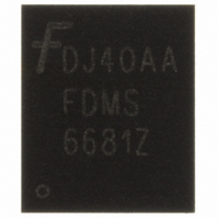
FDMS6681Z Fairchild Semiconductor, FDMS6681Z Datasheet - Page 3

FDMS6681Z
Manufacturer Part Number
FDMS6681Z
Description
MOSFET P-CH 30V 21.1A POWER56
Manufacturer
Fairchild Semiconductor
Series
PowerTrench®r
Datasheet
1.FDMS6681Z.pdf
(7 pages)
Specifications of FDMS6681Z
Fet Type
MOSFET P-Channel, Metal Oxide
Fet Feature
Logic Level Gate
Rds On (max) @ Id, Vgs
3.2 mOhm @ 22.1A, 10V
Drain To Source Voltage (vdss)
30V
Current - Continuous Drain (id) @ 25° C
21.1A
Vgs(th) (max) @ Id
3V @ 250µA
Gate Charge (qg) @ Vgs
241nC @ 10V
Input Capacitance (ciss) @ Vds
10380pF @ 15V
Power - Max
2.5W
Mounting Type
Surface Mount
Package / Case
8-PQFN, Power56
Configuration
Single Quad Drain Triple Source
Transistor Polarity
P-Channel
Resistance Drain-source Rds (on)
0.0035 Ohms
Drain-source Breakdown Voltage
- 30 V
Gate-source Breakdown Voltage
+/- 25 V
Continuous Drain Current
21.1 A
Power Dissipation
2.5 W
Maximum Operating Temperature
+ 150 C
Mounting Style
SMD/SMT
Minimum Operating Temperature
- 55 C
Lead Free Status / RoHS Status
Lead free / RoHS Compliant
Other names
FDMS6681ZTR
Available stocks
Company
Part Number
Manufacturer
Quantity
Price
Part Number:
FDMS6681Z
Manufacturer:
FAIRCHILD/仙童
Quantity:
20 000
©2009 Fairchild Semiconductor Corporation
FDMS6681Z Rev.C4
Typical Characteristics
1.6
1.4
1.2
1.0
0.8
0.6
90
75
60
45
30
15
90
75
60
45
30
15
Figure 3. Normalized On Resistance
0
Figure 1.
0
-75
Figure 5. Transfer Characteristics
0
0
PULSE DURATION = 80 s
DUTY CYCLE = 0.5% MAX
I
V
V
D
GS
-50
DS
= -22.1 A
vs Junction Temperature
-V
= -10 V
= -5 V
DS
PULSE DURATION = 80 s
DUTY CYCLE = 0.5% MAX
T
-25
,
J
On Region Characteristics
,
DRAIN TO SOURCE VOLTAGE (V)
-V
JUNCTION TEMPERATURE
1
GS
V
V
V
GS
GS
, GATE TO SOURCE VOLTAGE (V)
GS
0
1
= -4.5 V
= -10V
= -4 V
T
V
25
J
GS
= 25
T
= -3.5 V
2
J
50
= 150
T
o
C
J
= 25 °C unless otherwise noted
o
75
C
2
(
o
100 125 150
3
C
V
)
T
GS
J
= -55
= -3 V
o
C
3
4
3
0.001
0.01
100
0.1
12
10
1
9
6
3
0
5
4
3
2
1
0
Figure 2.
Figure 4.
Forward Voltage vs Source Current
0
0
2
vs Drain Current and Gate Voltage
Figure 6.
V
V
T
-V
GS
GS
J
0.2
SD
15
= 150
= 0 V
= -3 V
-V
, BODY DIODE FORWARD VOLTAGE (V)
Normalized On-Resistance
On-Resistance vs Gate to
GS
-I
Source Voltage
4
Source to Drain Diode
D
o
,
,
C
GATE TO SOURCE VOLTAGE (V)
DRAIN CURRENT (A)
0.4
30
PULSE DURATION = 80 s
DUTY CYCLE = 0.5%MAX
V
V
GS
GS
0.6
45
= -4.5 V
6
= -3.5 V
PULSE DURATION = 80 s
DUTY CYCLE = 0.5% MAX
T
T
J
J
= 125
= 25
0.8
60
o
o
C
T
C
T
J
J
8
= -55
= 25
V
www.fairchildsemi.com
I
V
GS
D
1.0
75
GS
= -22.1 A
o
= -10 V
o
C
C
= -4 V
1.2
90
10


