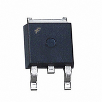
FDD3672 Fairchild Semiconductor, FDD3672 Datasheet - Page 5

FDD3672
Manufacturer Part Number
FDD3672
Description
MOSFET N-CH 100V 44A D-PAK
Manufacturer
Fairchild Semiconductor
Series
UltraFET™r
Type
Power MOSFETr
Datasheet
1.FDD3672.pdf
(11 pages)
Specifications of FDD3672
Fet Type
MOSFET N-Channel, Metal Oxide
Fet Feature
Standard
Rds On (max) @ Id, Vgs
28 mOhm @ 44A, 10V
Drain To Source Voltage (vdss)
100V
Current - Continuous Drain (id) @ 25° C
44A
Vgs(th) (max) @ Id
4V @ 250µA
Gate Charge (qg) @ Vgs
36nC @ 10V
Input Capacitance (ciss) @ Vds
1710pF @ 25V
Power - Max
135W
Mounting Type
Surface Mount
Package / Case
DPak, TO-252 (2 leads+tab), SC-63
Number Of Elements
1
Polarity
N
Channel Mode
Enhancement
Drain-source On-res
0.028Ohm
Drain-source On-volt
100V
Gate-source Voltage (max)
±20V
Drain Current (max)
6.5A
Power Dissipation
135W
Output Power (max)
Not RequiredW
Frequency (max)
Not RequiredMHz
Noise Figure
Not RequireddB
Power Gain
Not RequireddB
Drain Efficiency
Not Required%
Operating Temp Range
-55C to 175C
Operating Temperature Classification
Military
Mounting
Surface Mount
Pin Count
2 +Tab
Package Type
TO-252
Configuration
Single
Transistor Polarity
N-Channel
Resistance Drain-source Rds (on)
0.028 Ohm @ 10 V
Drain-source Breakdown Voltage
100 V
Gate-source Breakdown Voltage
+/- 20 V
Continuous Drain Current
6.5 A
Maximum Operating Temperature
+ 175 C
Mounting Style
SMD/SMT
Minimum Operating Temperature
- 55 C
Lead Free Status / RoHS Status
Lead free / RoHS Compliant
Other names
FDD3672
FDD3672TR
FDD3672TR
Available stocks
Company
Part Number
Manufacturer
Quantity
Price
Company:
Part Number:
FDD3672
Manufacturer:
FAIRCHILD
Quantity:
30 000
Part Number:
FDD3672
Manufacturer:
FAIRCHILD/仙童
Quantity:
20 000
©2010 Fairchild Semiconductor Corporation
Typical Characteristics
Breakdown Voltage vs Junction Temperature
10
1.2
1.1
1.0
0.9
8
6
4
2
0
Figure 11. Normalized Drain to Source
0
-80
Figure 13. Gate Charge Waveforms for
V
I
D
DD
= 250µA
= 50V
-40
5
T
J
, JUNCTION TEMPERATURE (
0
Constant Gate Currents
Q
g
, GATE CHARGE (nC)
10
40
80
WAVEFORMS IN
DESCENDING ORDER:
15
T
C
I
I
D
D
= 25°C unless otherwise noted
120
= 44A
= 21A
o
C)
20
160
200
25
3000
1000
Figure 12. Capacitance vs Drain to Source
100
200
100
10
0.1
10
1
0.1
1
THIS AREA IS
LIMITED BY r
C
C
OSS
V
RSS
GS
Figure 14. Forward Bias Safe
≅ C
= 0V, f = 1MHz
= C
V
SINGLE PULSE
T
R
T
V
DS
DS
J
C
GD
DS
JC
= MAX RATED
= 25
, DRAIN to SOURCE VOLTAGE (V)
+ C
, DRAIN TO SOURCE VOLTAGE (V)
DS(on)
= 1.11
Operating Area
GD
o
1
C
Voltage
o
10
C/W
C
ISS
10
= C
GS
+ C
100
GD
10 ms
1 ms
100 us
DC
FDD3672 Rev. A2
300
100


