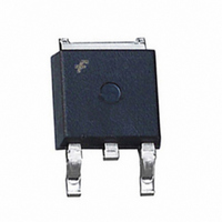
FDD5614P Fairchild Semiconductor, FDD5614P Datasheet - Page 2

FDD5614P
Manufacturer Part Number
FDD5614P
Description
MOSFET P-CH 60V 15A DPAK
Manufacturer
Fairchild Semiconductor
Series
PowerTrench®r
Type
Power MOSFETr
Datasheet
1.FDD5614P.pdf
(6 pages)
Specifications of FDD5614P
Fet Type
MOSFET P-Channel, Metal Oxide
Fet Feature
Logic Level Gate
Rds On (max) @ Id, Vgs
100 mOhm @ 4.5A, 10V
Drain To Source Voltage (vdss)
60V
Current - Continuous Drain (id) @ 25° C
15A
Vgs(th) (max) @ Id
3V @ 250µA
Gate Charge (qg) @ Vgs
24nC @ 10V
Input Capacitance (ciss) @ Vds
759pF @ 30V
Power - Max
1.6W
Mounting Type
Surface Mount
Package / Case
DPak, TO-252 (2 leads+tab), SC-63
Configuration
Single
Transistor Polarity
P-Channel
Resistance Drain-source Rds (on)
0.1 Ohm @ 10 V
Forward Transconductance Gfs (max / Min)
8 S
Drain-source Breakdown Voltage
60 V
Gate-source Breakdown Voltage
+/- 20 V
Continuous Drain Current
15 A
Power Dissipation
42000 mW
Maximum Operating Temperature
+ 175 C
Mounting Style
SMD/SMT
Minimum Operating Temperature
- 55 C
Number Of Elements
1
Polarity
P
Channel Mode
Enhancement
Drain-source On-res
0.1Ohm
Drain-source On-volt
60V
Gate-source Voltage (max)
±20V
Operating Temp Range
-55C to 175C
Operating Temperature Classification
Military
Mounting
Surface Mount
Pin Count
2 +Tab
Package Type
TO-252
Lead Free Status / RoHS Status
Lead free / RoHS Compliant
Other names
FDD5614PTR
Available stocks
Company
Part Number
Manufacturer
Quantity
Price
Company:
Part Number:
FDD5614P
Manufacturer:
FSC
Quantity:
12 000
Company:
Part Number:
FDD5614P
Manufacturer:
FAIRCHILD
Quantity:
25 016
Company:
Part Number:
FDD5614P
Manufacturer:
FSC
Quantity:
1 000
Company:
Part Number:
FDD5614P
Manufacturer:
FAIRCHILD
Quantity:
30 000
Part Number:
FDD5614P
Manufacturer:
FAIRCHILD/仙童
Quantity:
20 000
Electrical Characteristics
Symbol
Drain-Source Avalanche Ratings
W
I
Off Characteristics
BV
∆BV
I
I
I
On Characteristics
V
∆V
R
I
g
Dynamic Characteristics
C
C
C
Switching Characteristics
t
t
t
t
Q
Q
Q
Drain–Source Diode Characteristics and Maximum Ratings
I
V
AR
DSS
GSSF
GSSR
D(on)
d(on)
r
d(off)
f
S
FS
GS(th)
SD
∆T
∆T
DS(on)
iss
oss
rss
g
gs
gd
DSS
GS(th)
DSS
DSS
J
J
Single Pulse Drain-Source
Avalanche Energy
Maximum Drain-Source Avalanche
Current
Drain–Source Breakdown Voltage
Breakdown Voltage Temperature
Coefficient
Zero Gate Voltage Drain Current
Gate–Body Leakage, Forward
Gate–Body Leakage, Reverse
Gate Threshold Voltage
Gate Threshold Voltage
Temperature Coefficient
Static Drain–Source
On–Resistance
On–State Drain Current
Forward Transconductance
Input Capacitance
Output Capacitance
Reverse Transfer Capacitance
Turn–On Delay Time
Turn–On Rise Time
Turn–Off Delay Time
Turn–Off Fall Time
Total Gate Charge
Gate–Source Charge
Gate–Drain Charge
Maximum Continuous Drain–Source Diode Forward Current
Drain–Source Diode Forward
Voltage
Parameter
(Note 2)
(Note 2)
(Note 1)
V
I
V
V
V
V
I
V
V
V
V
V
V
f = 1.0 MHz
V
V
V
V
V
T
D
D
V
A
GS
DS
GS
GS
DS
GS
GS
GS
GS
DS
DS
DD
GS
DS
GS
GS
= –250 µA, Referenced to 25°C
= –250 µA, Referenced to 25°C
= 25°C unless otherwise noted
DD
= 0 V, I
= –48 V,
= 20V,
= –20 V,
= V
= –10 V,
= –4.5 V,
= –10 V,I
= –10 V,
= –5 V,
= –30 V,
= –30 V,
= –10 V,
= –30V,
= –10 V
= 0 V,
= –30 V,
Test Conditions
GS
, I
D
D
= –250 µA
I
= –250 µA
D
S
= –4.5 A,T
= –3.2 A
V
V
V
I
I
I
V
I
V
I
GS
DS
DS
D
D
D
D
I
R
D
D
DS
GS
= –4.5 A
= –4.5 A
= –3.9 A
= –3 A
GEN
= –4.5 A,
= 0 V
= 0 V
= 0 V
= –1 A,
= –5 V
= 0 V,
= 6 Ω
J
(Note 2)
=125°C
–60
Min
–20
–1
Typ Max Units
–1.6
–0.8
–49
137
759
2.5
3.0
76
99
90
39
10
19
12
15
4
8
7
–100
–4.5
–3.2
–1.2
100
100
130
185
90
–1
–3
14
20
34
22
24
FDD5614P Rev C1(W)
mV/°C
mV/°C
mΩ
mJ
nC
nC
nC
µA
nA
nA
pF
pF
pF
ns
ns
ns
ns
A
V
V
A
S
A
V


