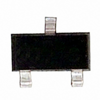
NDS355AN Fairchild Semiconductor, NDS355AN Datasheet - Page 6

NDS355AN
Manufacturer Part Number
NDS355AN
Description
MOSFET N-CH 30V 1.7A SSOT3
Manufacturer
Fairchild Semiconductor
Datasheet
1.NDS355AN.pdf
(7 pages)
Specifications of NDS355AN
Fet Type
MOSFET N-Channel, Metal Oxide
Fet Feature
Logic Level Gate
Rds On (max) @ Id, Vgs
85 mOhm @ 1.9A, 10V
Drain To Source Voltage (vdss)
30V
Current - Continuous Drain (id) @ 25° C
1.7A
Vgs(th) (max) @ Id
2V @ 250µA
Gate Charge (qg) @ Vgs
5nC @ 5V
Input Capacitance (ciss) @ Vds
195pF @ 15V
Power - Max
460mW
Mounting Type
Surface Mount
Package / Case
3-SSOT, SuperSOT-3
Configuration
Single
Transistor Polarity
N-Channel
Resistance Drain-source Rds (on)
0.085 Ohm @ 10 V
Drain-source Breakdown Voltage
30 V
Gate-source Breakdown Voltage
+/- 20 V
Continuous Drain Current
1.7 A
Power Dissipation
500 mW
Maximum Operating Temperature
+ 150 C
Mounting Style
SMD/SMT
Minimum Operating Temperature
- 55 C
Lead Free Status / RoHS Status
Lead free / RoHS Compliant
Other names
NDS355ANTR
Available stocks
Company
Part Number
Manufacturer
Quantity
Price
Company:
Part Number:
NDS355AN
Manufacturer:
FS8
Quantity:
48 000
Part Number:
NDS355AN
Manufacturer:
FAIRCHILD/仙童
Quantity:
20 000
Part Number:
NDS355AN-NL
Manufacturer:
FAIRCHILD/仙童
Quantity:
20 000
Typical Electrical Characteristics
0.8
0.6
0.4
0.2
Steady-State Power Dissipation versus Copper
0.005
0.002
0.001
7
6
5
4
3
2
1
0
Figure 13. Transconductance Variation with Drain
1
0
0.05
0.02
0.01
0
0.5
0.2
0.1
0
0.0001
Figue 15. SuperSOT
1
1b
1a
V
D = 0.5
DS
0.05
0.02
0.01
0.2
0.1
= 5.0V
2
Single Pulse
2oz COPPER MOUNTING PAD AREA (in )
0.1
Mounting Pad Area.
Figure 17. Transient Thermal Response Curve.
Note : Characterization performed using the conditions described in note 1b. Transient thermal response will
Current and Temperature
I , DRAIN CURRENT (A)
D
0.001
change depending on the circuit board design.
4
TM _
0.2
3 Maximum
6
T = -55°C
J
125°C
25°C
0.01
0.3
(continued)
4.5"x5" FR-4 Board
T = 25 C
Still Air
A
2
8
.
o
0.4
10
0.1
t , TIME (sec)
1
0.03
0.01
0.3
0.1
Figure 14. Maximum Safe Operating Area
30
10
1.8
1.6
1.4
1.2
5
3
1
0.1
2
0
Current versus Copper Mounting Pad Area
1b
Figure 16. Maximum Steady-State Drain
1a
R
0.2
SINGLE PULSE
JA
V
T = 25°C
=See Note1b
GS
A
1
= 4.5V
2oz COPPER MOUNTING PAD AREA (in )
V
0.5
0.1
DS
, DRAI N-SOURCE VOLTAGE (V)
1
P(pk)
2
T - T
R
R
Duty Cycle, D = t /t
0.2
J
10
JA
JA
t
1
A
(t) = r(t) * R
= See Note 1b
t
= P * R
5
2
4.5"x5" FR-4 Board
T = 25 C
Still Air
V
10
A
GS
JA
= 4.5V
0.3
1
(t)
2
JA
o
2
20 30
.
100
NDS355AN Rev.C
.
50
0.4
300


