FDC6302P Fairchild Semiconductor, FDC6302P Datasheet - Page 2
FDC6302P
Manufacturer Part Number
FDC6302P
Description
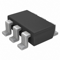
MOSFET P-CH DUAL 25V SSOT6
Manufacturer
Fairchild Semiconductor
Datasheet
1.FDC6302P.pdf
(5 pages)
Specifications of FDC6302P
Fet Type
2 P-Channel (Dual)
Fet Feature
Logic Level Gate
Rds On (max) @ Id, Vgs
10 Ohm @ 200mA, 4.5V
Drain To Source Voltage (vdss)
25V
Current - Continuous Drain (id) @ 25° C
120mA
Vgs(th) (max) @ Id
1.5V @ 250µA
Gate Charge (qg) @ Vgs
0.31nC @ 4.5V
Input Capacitance (ciss) @ Vds
11pF @ 10V
Power - Max
700mW
Mounting Type
Surface Mount
Package / Case
6-SSOT, SuperSOT-6
Configuration
Dual
Transistor Polarity
P-Channel
Resistance Drain-source Rds (on)
10 Ohm @ 4.5 V
Forward Transconductance Gfs (max / Min)
0.135 S
Drain-source Breakdown Voltage
25 V
Gate-source Breakdown Voltage
8 V
Continuous Drain Current
0.12 A
Power Dissipation
900 mW
Maximum Operating Temperature
+ 150 C
Mounting Style
SMD/SMT
Minimum Operating Temperature
- 55 C
Continuous Drain Current Id
-200mA
Drain Source Voltage Vds
-25V
On Resistance Rds(on)
10ohm
Rds(on) Test Voltage Vgs
-4.5V
Threshold Voltage Vgs Typ
-1V
Rohs Compliant
Yes
Lead Free Status / RoHS Status
Lead free / RoHS Compliant
Available stocks
Company
Part Number
Manufacturer
Quantity
Price

Part Number:
FDC6302P
Manufacturer:
FAIRCHILD/仙童
Quantity:
20 000
Part Number:
FDC6302P-NL
Manufacturer:
FAIRCHILD/仙童
Quantity:
20 000


Electrical Characteristics
Symbol
OFF CHARACTERISTICS
BV
I
I
ON CHARACTERISTICS
V
R
I
g
DYNAMIC CHARACTERISTICS
C
C
C
SWITCHING CHARACTERISTICS
t
t
t
t
Q
Q
Q
DRAIN-SOURCE DIODE CHARACTERISTICS AND MAXIMUM RATINGS
I
V
Notes:
1. R
2. Pulse Test: Pulse Width < 300µs, Duty Cycle < 2.0%.
DSS
GSS
D(ON)
D(on)
r
D(off)
f
S
FS
BV
V
GS(th)
SD
DS(ON)
iss
oss
rss
g
gs
gd
DSS
GS(th)
design while R
DSS
JA
is the sum of the junction-to-case and case-to-ambient thermal resistance where the case thermal reference is defined as the solder mounting surface of the drain pins. R
/ T
/ T
J
J
a. 140
2oz copper.
CA
Parameter
Drain-Source Breakdown Voltage
Breakdown Voltage Temp. Coefficient
Zero Gate Voltage Drain Current
Gate - Body Leakage Current
Gate Threshold Voltage Temp. Coefficient
Gate Threshold Voltage
Static Drain-Source On-Resistance
On-State Drain Current
Forward Transconductance
Input Capacitance
Output Capacitance
Reverse Transfer Capacitance
Turn - On Delay Time
Turn - On Rise Time
Turn - Off Delay Time
Turn - Off Fall Time
Total Gate Charge
Gate-Source Charge
Gate-Drain Charge
Maximum Continuous Drain-Source Diode Forward Current
Drain-Source Diode Forward Voltage
is determined by the user's board design.
O
C/W on a 0.125 in
(Note 2)
2
pad of
(Note 2)
(T
A
= 25
O
C unless otherwise noted )
b. 180
of 2oz copper.
O
C/W on a 0.005 in
Conditions
V
I
V
V
I
V
V
V
V
V
V
V
V
V
V
V
D
D
f = 1.0 MHz
GS
DS
GS
DS
GS
GS
GS
DS
DS
DD
GS
DS
GS
GS
= -250 µA, Referenced to 25
= -250 µA, Referenced to 25
= -20 V, V
= V
= -5 V, I
= -10 V, V
= -5 V, I
= 0 V, I
= -8 V, V
= -2.7 V, I
= -4.5 V, I
= -2.7 V, V
= -6 V, I
= -4.5 V, R
= -4.5 V
= 0 V, I
2
of pad
GS
, I
D
D
S
D
D
D
= -250 µA
= -0.7 A
= -250 µA
DS
= -0.2 A
= - 0.2 A,
D
D
GS
GS
= -0.2 A,
= 0 V
DS
GEN
= -0.05A
= -0.2 A
= 0 V
= 0 V,
= -5 V
= 50
(Note 2)
T
T
J
J
= 55°C
=125°C
o
o
C
C
-0.65
-0.05
Min
-25
0.135
10.6
0.22
0.12
0.05
Typ
-20
1.9
7.9
1.4
12
11
-1
-1
7
5
8
9
5
Max
-100
0.31
-1.5
-0.7
-1.3
JC
-10
13
10
18
12
16
18
10
-1
is guaranteed by
FDC6302P Rev.C
mV /
mV /
Units
µA
µA
nC
nC
nC
nA
ns
ns
ns
ns
V
V
A
S
A
V
pF
pF
pF
o
o
C
C
Related parts for FDC6302P
Image
Part Number
Description
Manufacturer
Datasheet
Request
R

Part Number:
Description:
Fairchild Semiconductor [IGBT MODULE]
Manufacturer:
Fairchild Semiconductor
Datasheet:

Part Number:
Description:
Discrete Semiconductor Modules
Manufacturer:
Fairchild Semiconductor
Part Number:
Description:
Discrete Semiconductor Modules
Manufacturer:
Fairchild Semiconductor
Part Number:
Description:
This N-Channel MOSFET is produced using Fairchild Semiconductor’s advanced Power Trench® process
Manufacturer:
Fairchild Semiconductor
Datasheet:
Part Number:
Description:
This N-Channel MOSFET is produced using Fairchild Semiconductor’s advanced Power Trench® process
Manufacturer:
Fairchild Semiconductor
Datasheet:
Part Number:
Description:
This N-Channel MOSFET is produced using Fairchild Semiconductor’s advanced PowerTrench® process
Manufacturer:
Fairchild Semiconductor
Datasheet:
Part Number:
Description:
This N-Channel MOSFET is produced using Fairchild Semiconductor’s advanced PowerTrench® process
Manufacturer:
Fairchild Semiconductor
Datasheet:
Part Number:
Description:
This N-Channel MOSFET is produced using Fairchild Semiconductor’s advanced Power Trench® process
Manufacturer:
Fairchild Semiconductor
Datasheet:
Part Number:
Description:
This N-Channel logic Level MOSFETs are produced using Fairchild Semiconductor‘s advanced Power Trench® process that has been special tailored to minimize the on-state resistance and yet maintain superior switching performance
Manufacturer:
Fairchild Semiconductor
Datasheet:
Part Number:
Description:
This N-Channel MOSFET is produced using Fairchild Semiconductor’s advanced Power Trench® process
Manufacturer:
Fairchild Semiconductor
Datasheet:
Part Number:
Description:
This N-Channel SyncFET™ is produced using Fairchild Semiconductor’s advanced PowerTrench® process
Manufacturer:
Fairchild Semiconductor
Datasheet:
Part Number:
Description:
This N-Channel SyncFET™ is produced using Fairchild Semiconductor’s advanced PowerTrench® process
Manufacturer:
Fairchild Semiconductor
Datasheet:
Part Number:
Description:
This N-Channel SyncFET™ is produced using Fairchild Semiconductor’s advanced PowerTrench® process
Manufacturer:
Fairchild Semiconductor
Datasheet:
Part Number:
Description:
This N-Channel logic Level MOSFETs are produced using Fairchild Semiconductor‘s advanced Power Trench® process that has been special tailored to minimize the on-state resistance and yet maintain superior switching performance
Manufacturer:
Fairchild Semiconductor
Datasheet:
Part Number:
Description:
This N-Channel MOSFET is produced using Fairchild Semiconductor’s advanced Power Trench® process that has been especially tailored to minimize the on-state resistance and yet maintain superior switching performance
Manufacturer:
Fairchild Semiconductor
Datasheet: